
What are Schottky Barrier Diodes (SBD)?
Schottky barrier diodes (SBDs) are a special kind of diode that you and I use when we need fast response times and low power loss. Unlike regular diodes that rely on a p-n junction, these diodes are built using a metal-semiconductor junction. This forms what we call a Schottky barrier — a potential barrier that helps current flow more efficiently. Because of this unique structure, we get much faster switching speeds and lower forward voltage drops than what you’d typically see with standard diodes. So, whether we’re designing power circuits or high-speed electronics, Schottky diodes offer clear advantages that can really make a difference in performance.
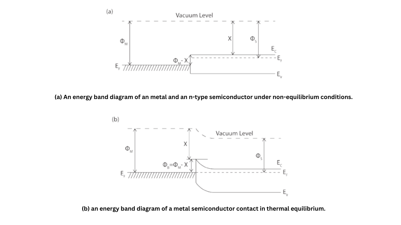
When you bring a metal or superconductor into close contact with a semiconductor, the Fermi levels in both materials must be equal at thermal equilibrium. Additionally, the vacuum level must remain continuous across the interface. These two requirements lead to a unique energy band diagram for the contact, as shown in Figure 1.
The Schottky Barrier
At the interface, the resulting band bending creates a potential barrier known as the Schottky barrier. The height of this barrier, denoted as ΦBn\Phi_{Bn}, is the difference between the metal work function (Φm\Phi_m), which represents the energy difference between the metal Fermi level and the vacuum level, and the electron affinity (χ\chi) of the semiconductor, which represents the difference between the semiconductor’s conduction band edge and the vacuum level.
Adjusting the Schottky Barrier
The width of the Schottky barrier depends on various factors, including the doping density of the semiconductor. In semiconductor-superconductor-semiconductor (SSmS) junctions, you can adjust the barrier to allow either more or fewer electrons to tunnel through it by changing the doping density.
In Summary
The Schottky barrier forms at the interface between a metal or superconductor and a semiconductor due to the alignment of Fermi levels and the continuity of the vacuum level. The barrier height is determined by the difference between the metal work function and the semiconductor’s electron affinity. By tuning the doping density of the semiconductor, you can control the width of the barrier and thus manage electron tunneling through the junction