Close Menu
  • Analog Design
    • Latest Analog Layout Interview Questions (2025)
  • Digital Design
    • Digital Electronics Interview Question(2025)
    • Top VLSI Interview Questions
  • Physical Design
    • Physical Design Interview Questions for VLSI Engineers
  • Verilog
    • Verilog Interview Questions(2024)
  • Forum
Facebook Instagram YouTube LinkedIn WhatsApp
SiliconvlsiSiliconvlsi
Forum Questions Register in Forum Login in Forum
Facebook Instagram YouTube LinkedIn WhatsApp
  • Analog Design
    • Latest Analog Layout Interview Questions (2025)
  • Digital Design
    • Digital Electronics Interview Question(2025)
    • Top VLSI Interview Questions
  • Physical Design
    • Physical Design Interview Questions for VLSI Engineers
  • Verilog
    • Verilog Interview Questions(2024)
  • Forum
SiliconvlsiSiliconvlsi
Home»VLSI Design»What is a soft check or a stamping conflict at LVS?
VLSI Design

What is a soft check or a stamping conflict at LVS?

siliconvlsiBy siliconvlsiJanuary 12, 2022Updated:May 12, 2024No Comments2 Mins Read
Facebook Pinterest LinkedIn Email WhatsApp
Share
Facebook Twitter LinkedIn Pinterest Email

Soft check or a Stamping conflict at LVS?

Soft check or  Stamping conflict Error comes under ERC check. Soft Connect is a node connected through a Highly resistive non-routing layer that leads to poor circuit performance.

This soft check will identify shorts between two or more signals passing through high-resistivity materials such as n-well and p-substrate.

 It will come when two or more nets are connected with a high resistive layer (well ).

  • If Tap is not connected with power or ground then also it will flag(Floating well or floating p-substrate)
  • If  Two Nwell is connected in series by Nwell tap through the metal
  • If there are any layout nodes with a different name that are connected through some high resistive layers like n-well or p-well substrates then this soft check reports them.
In summary, the main difference between “Stamping conflict” and “Sconnect error” in LVS is that stamping conflicts are primarily concerned with how layout cells are instantiated and organized, while Sconnect errors focus on discrepancies in the electrical connectivity between the layout and the schematic representation of the IC design. Both types of errors are critical to identify and resolve to ensure the accurate and functional implementation of the integrated circuit.
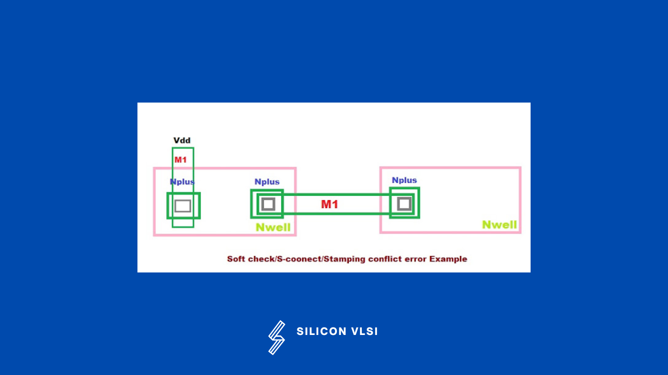
stamping conflict
stamping conflict.


Share. Facebook Twitter Pinterest LinkedIn Tumblr Email

Related Posts

How Shielding Avoids Crosstalk Problem? What Exactly Happens There?

September 22, 2024

Navigating the Challenges of Gate Dielectric Scaling in MOS Transistors

August 1, 2024

Challenges in Modern SoC Design Verification

April 20, 2024
Leave A Reply Cancel Reply

Facebook X (Twitter) Instagram Pinterest Vimeo YouTube
  • About Us
  • Contact Us
  • Privacy Policy
© 2025 Siliconvlsi.

Type above and press Enter to search. Press Esc to cancel.