Close Menu
  • Analog Design
    • Latest Analog Layout Interview Questions (2025)
  • Digital Design
    • Digital Electronics Interview Question(2025)
    • Top VLSI Interview Questions
  • Physical Design
    • Physical Design Interview Questions for VLSI Engineers
  • Verilog
    • Verilog Interview Questions(2024)
  • Forum
Facebook Instagram YouTube LinkedIn WhatsApp
SiliconvlsiSiliconvlsi
Forum Questions Register in Forum Login in Forum
Facebook Instagram YouTube LinkedIn WhatsApp
  • Analog Design
    • Latest Analog Layout Interview Questions (2025)
  • Digital Design
    • Digital Electronics Interview Question(2025)
    • Top VLSI Interview Questions
  • Physical Design
    • Physical Design Interview Questions for VLSI Engineers
  • Verilog
    • Verilog Interview Questions(2024)
  • Forum
SiliconvlsiSiliconvlsi
Home»VLSI Design»What is EPI in Silicon VLSI Technology?
VLSI Design

What is EPI in Silicon VLSI Technology?

siliconvlsiBy siliconvlsiJanuary 18, 2022Updated:June 4, 2024No Comments1 Min Read
Facebook Pinterest LinkedIn Email WhatsApp
Share
Facebook Twitter LinkedIn Pinterest Email

What is EPI in Silicon VLSI Technology?

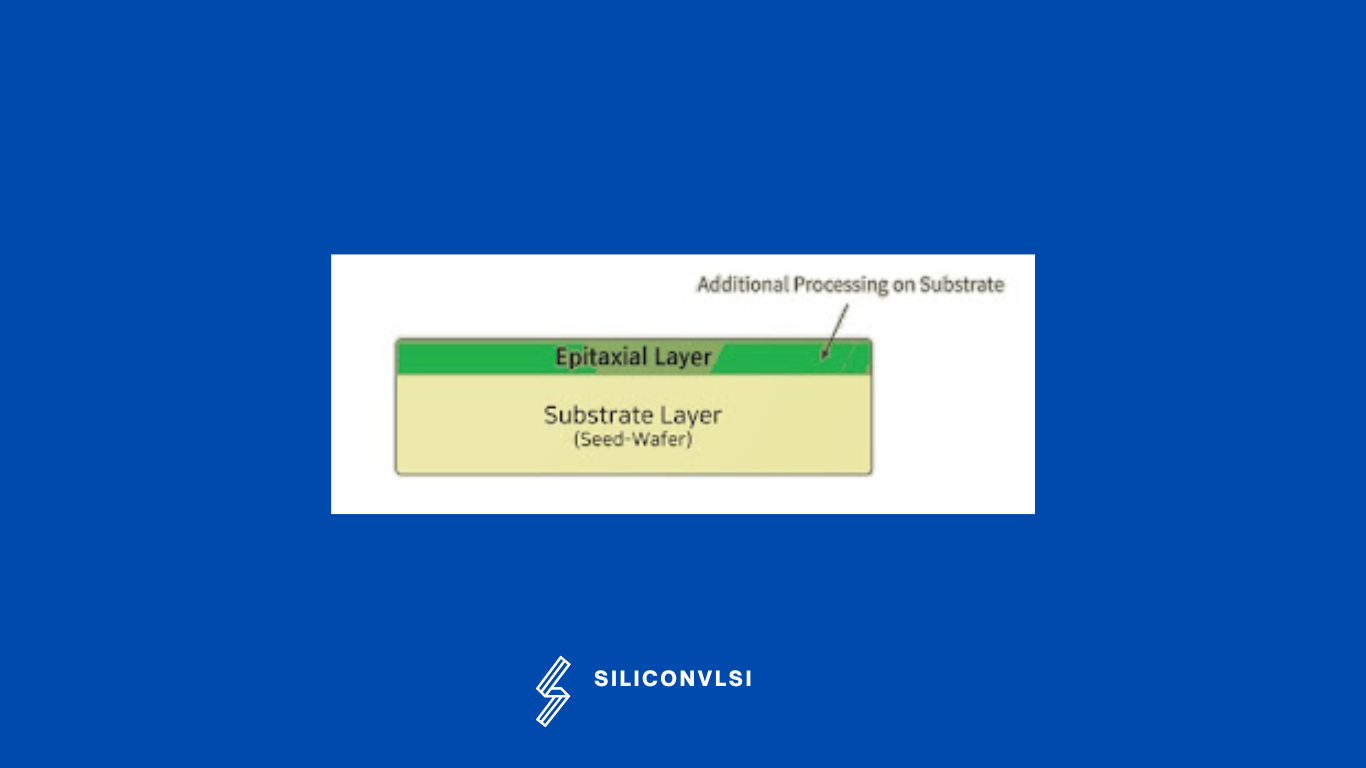
EPI stands for Epitaxial Silicon layer. The EPI layer is doped appropriately for the best transistor performance which means more lightly doped than the remaining lower portion of the substrate that is highly doped. 

Epitaxial Silicon layer

The highly doped substrate directs majority carriers to the ground and reflects minority carriers making the guard rings more effective.

This Epitaxial Silicon layer helps to avoid the Latch-up problem in CMOS VLSI technology.

Epitaxial Silicon Wafer for IC and Power Applications

Silicon epitaxy is a complex process where an additional layer of monocrystalline silicon is deposited onto the polished surface of a silicon wafer. Unlike simple epitaxy, silicon epitaxy involves multiple simultaneous chemical reactions. During epitaxial layer growth, chemical substances are deposited on top of an existing crystal layer, resulting in layered growth, also known as “stacking.” Silicon-based devices can be fabricated using this process, with layers formed in two different directions.

Share. Facebook Twitter Pinterest LinkedIn Tumblr Email

Related Posts

How Shielding Avoids Crosstalk Problem? What Exactly Happens There?

September 22, 2024

Navigating the Challenges of Gate Dielectric Scaling in MOS Transistors

August 1, 2024

Challenges in Modern SoC Design Verification

April 20, 2024
Leave A Reply Cancel Reply

Facebook X (Twitter) Instagram Pinterest Vimeo YouTube
  • About Us
  • Contact Us
  • Privacy Policy
© 2025 Siliconvlsi.

Type above and press Enter to search. Press Esc to cancel.