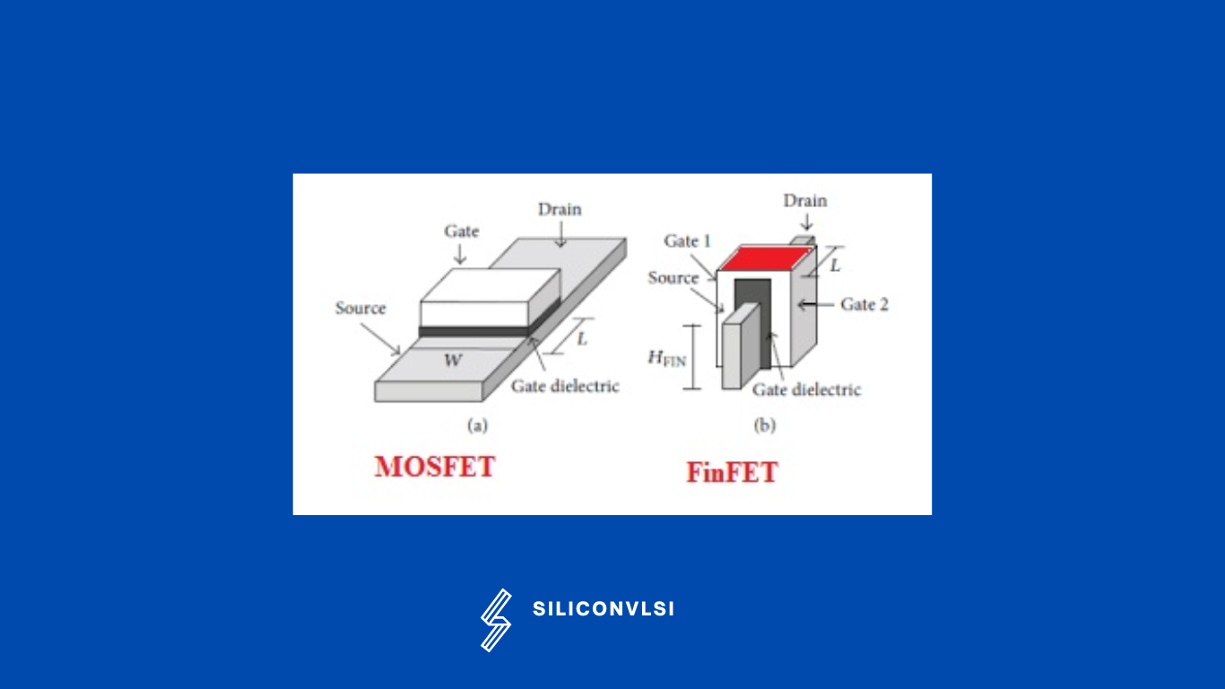
Close Menu
  • Analog Design
    • Latest Analog Layout Interview Questions (2025)
  • Digital Design
    • Digital Electronics Interview Question(2025)
    • Top VLSI Interview Questions
  • Physical Design
    • Physical Design Interview Questions for VLSI Engineers
  • Verilog
    • Verilog Interview Questions(2024)
  • Forum
Facebook Instagram YouTube LinkedIn WhatsApp
SiliconvlsiSiliconvlsi
Ask Questions Register in Forum Login in Forum
Facebook Instagram YouTube LinkedIn WhatsApp
  • Analog Design
    • Latest Analog Layout Interview Questions (2025)
  • Digital Design
    • Digital Electronics Interview Question(2025)
    • Top VLSI Interview Questions
  • Physical Design
    • Physical Design Interview Questions for VLSI Engineers
  • Verilog
    • Verilog Interview Questions(2024)
  • Forum
SiliconvlsiSiliconvlsi
Home»VLSI Design»What is FinFET Technology
VLSI Design

What is FinFET Technology

siliconvlsiBy siliconvlsiMarch 31, 2022Updated:June 28, 2025No Comments1 Min Read
Facebook Pinterest LinkedIn Email WhatsApp
Share
Facebook Twitter LinkedIn Pinterest Email

FinFET Technology

Nowadays, FinFET technology is being adopted in a variety of forms by IC manufacturers who need to increase the density of their ICs without using such small feature sizes that the device performance falls. As a result, FinFET transistor technology has enabled the development of IC technology and it has a great PPA performance.

FinFET Technology
FinFET Technology

FinFET advantages and disadvantages

FinFET advantages 

FinFETs have several key advantages that make them ideal for use in applications.

  • Better channel control
  • No DIBL effect
  • Suppression of short-channel effects
  • Faster switching speed
  • Higher drain current
  • Less Second order effect
  • Lower switching voltage
  • Lower power consumption

FinFET disadvantages 

  • Difficult to control voltage threshold
  • No Body bias effect
  • A three-dimensional profile leads to higher parasitic
  • Very high capacitances
  • High fabrication cost

Share. Facebook Twitter Pinterest LinkedIn Tumblr Email

Related Posts

How Shielding Avoids Crosstalk Problem? What Exactly Happens There?

September 22, 2024

Navigating the Challenges of Gate Dielectric Scaling in MOS Transistors

August 1, 2024

Challenges in Modern SoC Design Verification

April 20, 2024
Leave A Reply Cancel Reply

Facebook X (Twitter) Instagram Pinterest Vimeo YouTube
  • About Us
  • Contact Us
  • Privacy Policy
© 2025 Siliconvlsi.

Type above and press Enter to search. Press Esc to cancel.