
Close Menu
  • Analog Design
    • Latest Analog Layout Interview Questions
  • Digital Design
    • Digital Electronics Interview Question
    • Top VLSI Interview Questions
  • Physical Design
    • Physical Design Interview Questions for VLSI Engineers
  • Verilog
    • Verilog Interview Questions(2026)
  • Forum
  • Calculators
    • Asynchronous FIFO Depth Calculator
    • Clock Skew and Clock Jitter Calculator
    • Setup Time Calculator
Facebook Instagram YouTube LinkedIn WhatsApp
SiliconvlsiSiliconvlsi
Ask Questions Register in Forum Login in Forum
Facebook Instagram YouTube LinkedIn WhatsApp
  • Analog Design
    • Latest Analog Layout Interview Questions
  • Digital Design
    • Digital Electronics Interview Question
    • Top VLSI Interview Questions
  • Physical Design
    • Physical Design Interview Questions for VLSI Engineers
  • Verilog
    • Verilog Interview Questions(2026)
  • Forum
  • Calculators
    • Asynchronous FIFO Depth Calculator
    • Clock Skew and Clock Jitter Calculator
    • Setup Time Calculator
SiliconvlsiSiliconvlsi
Home ยป NBTI in Semiconductor Devices and VLSI Design
Digital Design

NBTI in Semiconductor Devices and VLSI Design

siliconvlsiBy siliconvlsiOctober 1, 2022Updated:January 11, 2025No Comments2 Mins Read
Facebook Pinterest LinkedIn Email WhatsApp
Share
Facebook Twitter LinkedIn Pinterest Email

Table of Contents

Toggle
  • Negative bias temperature instability
    • What is the difference between NBTI and PBTI?

Negative bias temperature instability

When we applied a Negative voltage to the gate, dangling bonds called traps developed between the si-sio2 surface. This is called an NBTI. This is also called the aging effect.
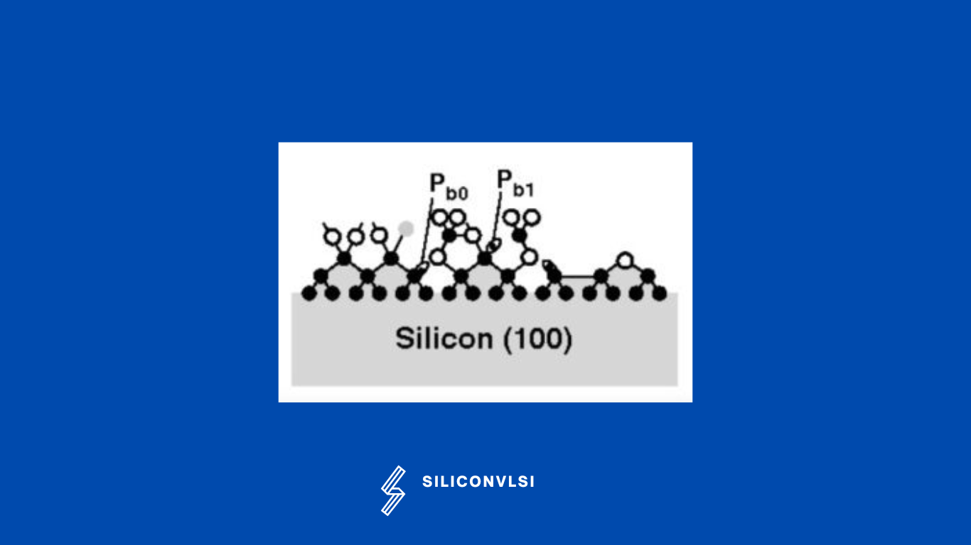
 

Important device parameters, such as the threshold voltage, are seen to change over time in a modern PMOS device when the gate voltage is driven below its source voltage. In the past, it has been hypothesized that the shift is caused by both the trapping of holes in oxide defects and the formation of interface states.

Due to time- and temperature-dependent changes in device characteristics throughout both on and off states of operation, NBTI can be a serious reliability issue in SiO2 gate dielectrics. Although NBTI is also present in NMOS devices, it is far more noticeable in PMOS transistors.
Negative-bias temperature instability (NBTI)


What is the difference between NBTI and PBTI?

As pMOSFETs and nMOSFETs are activated by negative and positive gate bias, respectively, Negative Bias Temperature Instability (NBTI) predominantly affects pMOSFETs, whereas Positive Bias Temperature Instability (PBTI) predominantly affects nMOSFETs. The significance of PBTI compared to NBTI depends on the manufacturing process, and their effects on circuits can accumulate rather than offsetting each other.


Share. Facebook Twitter Pinterest LinkedIn Tumblr Email

Related Posts

Voltage-Aware DRC: 7 Essential Concepts for Reliable Signoff

September 14, 2026

Difference Between Clipper and Clamper

June 22, 2025

What is difference Between RAM Bandwidth and Clock Speed

December 1, 2024
Leave A Reply Cancel Reply

Facebook X (Twitter) Instagram Pinterest Vimeo YouTube
  • About Us
  • Contact Us
  • Privacy Policy
© 2026 Siliconvlsi.

Type above and press Enter to search. Press Esc to cancel.