
What is a Stick Diagram In VLSI?
A stick diagram is a diagrammatic representation of a chip layout that helps to abstract a model. Stick diagrams are used to convey the layer information with the help of a color code.
“A stick diagram is a cartoon of a layout!!!”
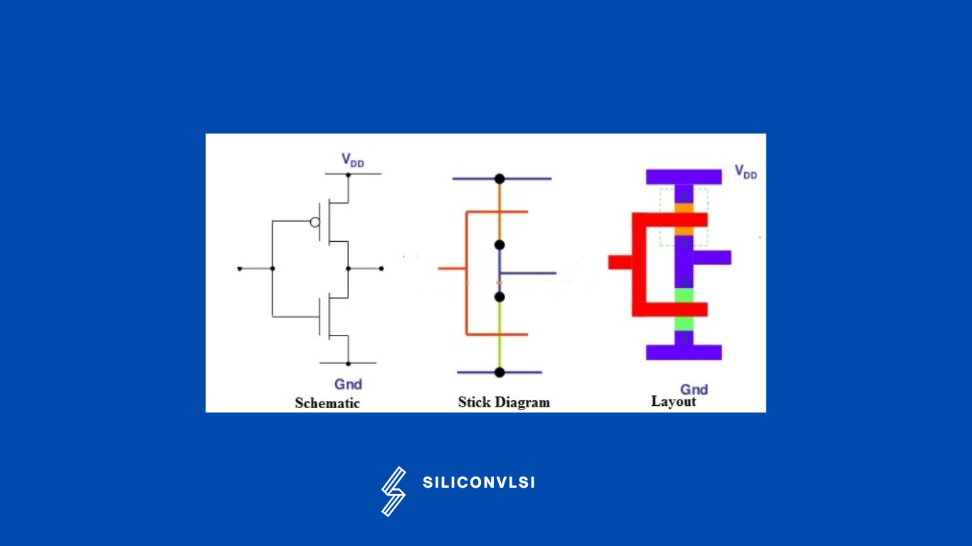
The CMOS layout can also be created using Stick diagrams. In these diagrams, designers sketch a layout by hand, using colored lines to represent different process layers like diffusion, metal, and polysilicon.
The designer draws a freehand sketch of a layout, using colored lines to represent the various process layers such as diffusion, metal, and polysilicon.
For example, in the case of nMOS design,
• Red color is used for n-diffusion
• Green for polysilicon
• Blue for metal
• Yellow for an implant, and black for contact areas.
Stick Diagrams Rules
If the same layer crosses each other, it makes contact.
If the different layers just cross, it doesn’t make contact but if contact has to be made, it must be in the form of a dark-shaded circle.
If polysilicon crosses the n-type of diffusion, then the nMOS enhancement transistor is formed.
Cross mark has to be used on Vdd and Vss rails in order to create n-well and p-well contact for PMOS devices and NMOS devices respectively.
PMOS devices must be placed in the pull-up part(above the line) and NMOS devices in the pull-down part(below the line) in the CMOS design style.