
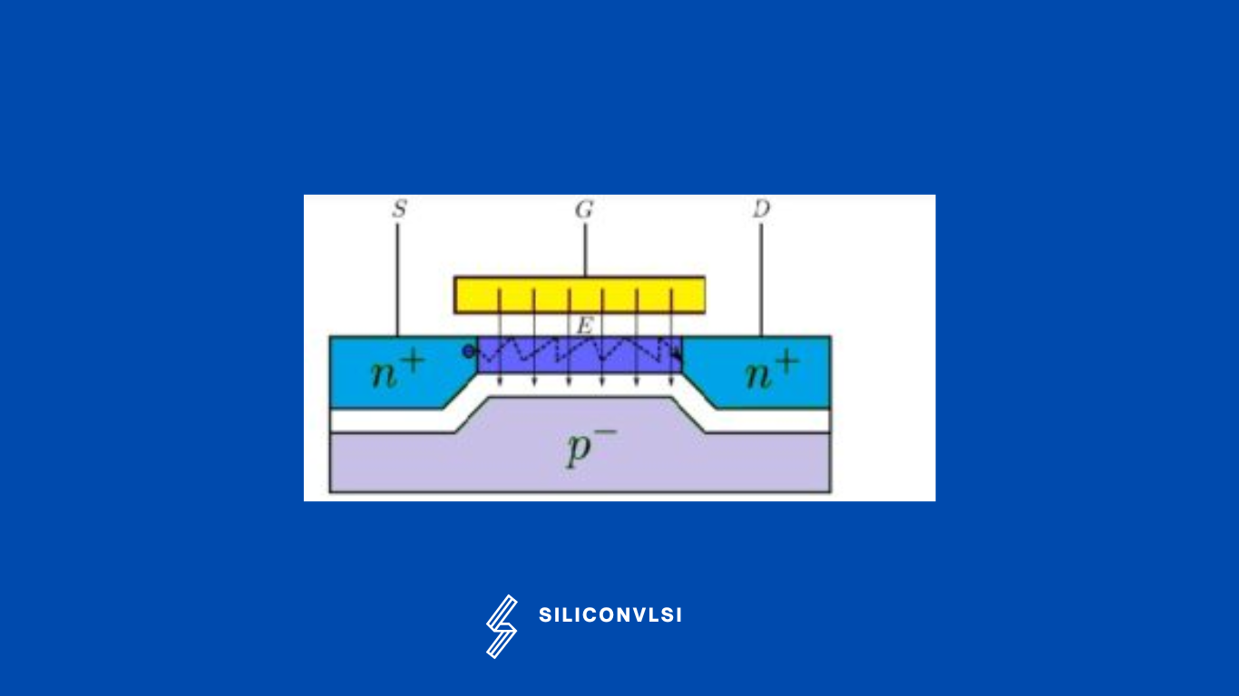
Surface scattering in MOSFET
Surface scattering occurs when electrons are accelerated toward the surface by the vertical component of the electric field and due to its reduction in mobility. The electrons are attracted by the positive Gate field; They keep bouncing and crashing against the oxide surface. This reduces the mobility of the carriers. For example just like you are crowded in a railway station, where you cannot travel faster due to the random movement of passengers. A reduction in carrier mobility means a reduction in the current.
Types of Short-Channel Effects
- Drain-induced barrier lowering
- Punch through
- Surface scattering
- Velocity saturation
- Impact ionization
- Hot electrons