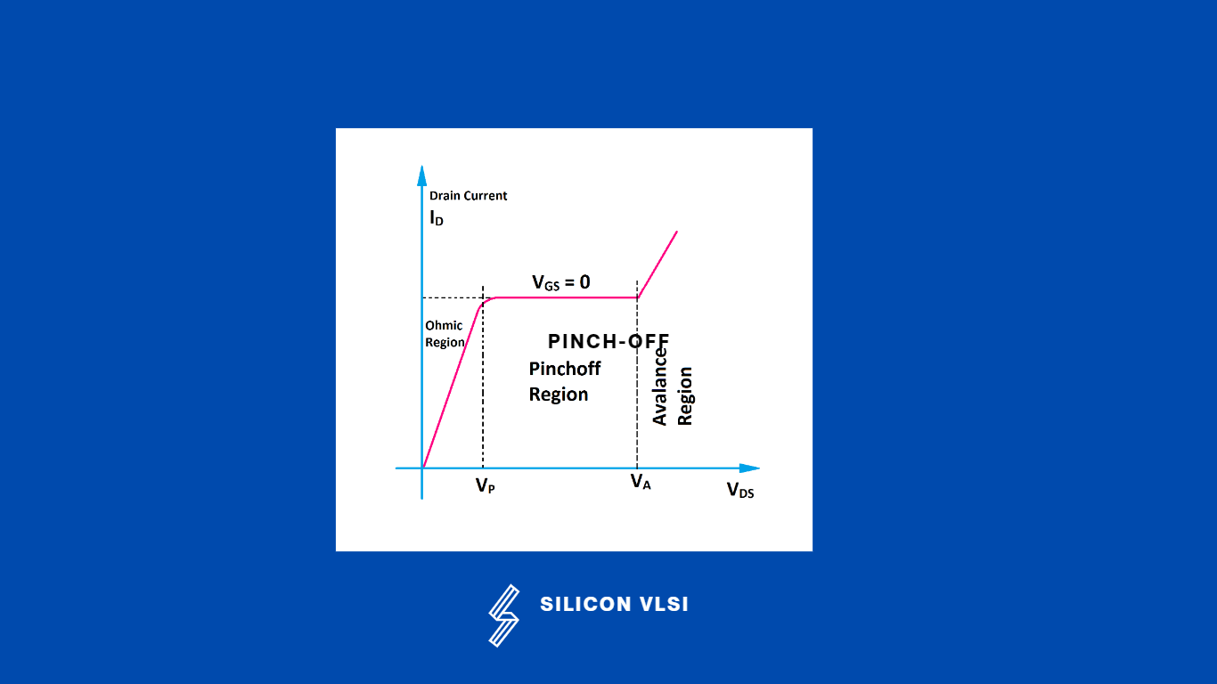
“Pinch-off happens during saturation mode because of the strong electric fields that are generated within the channel region when a voltage is applied to the gate of the transistor.”
What is Pinch-off
When the voltage applied to the gate exceeds the threshold voltage of the transistor, the channel is induced and a current begins to flow between the source and drain terminals. As the voltage applied to the gate is increased further, the channel region becomes narrower due to the accumulation of charges on the gate oxide layer.
At some point, the channel width becomes so narrow that the electric field within the channel is strong enough to completely deplete the region of mobile charge carriers (electrons or holes) near the drain side of the channel. This region becomes known as the pinch-off region.
As the pinch-off region becomes wider, the drain current remains constant and the saturation region of the transistor is reached. At this point, the drain current is limited by the resistance of the pinch-off region and the voltage drop across it. The pinch-off region acts like a resistor, and the saturation current is proportional to the channel width at the pinch-off region.
Effect of Pinch off
The pinch-off region can limit the performance of CMOS devices because it can introduce non-linearities and limit the maximum drain current that can be achieved in the saturation region. Therefore, circuit designers need to carefully optimize the device dimensions and operating conditions to minimize the effects of pinch-off and achieve the desired performance characteristics.
- VDS – Voltage across Drain to Source
- VGS – Voltage Across Gate to Source
- Pinch Off – Voltage across the drain to source when Drain Current constant and VGS = 0
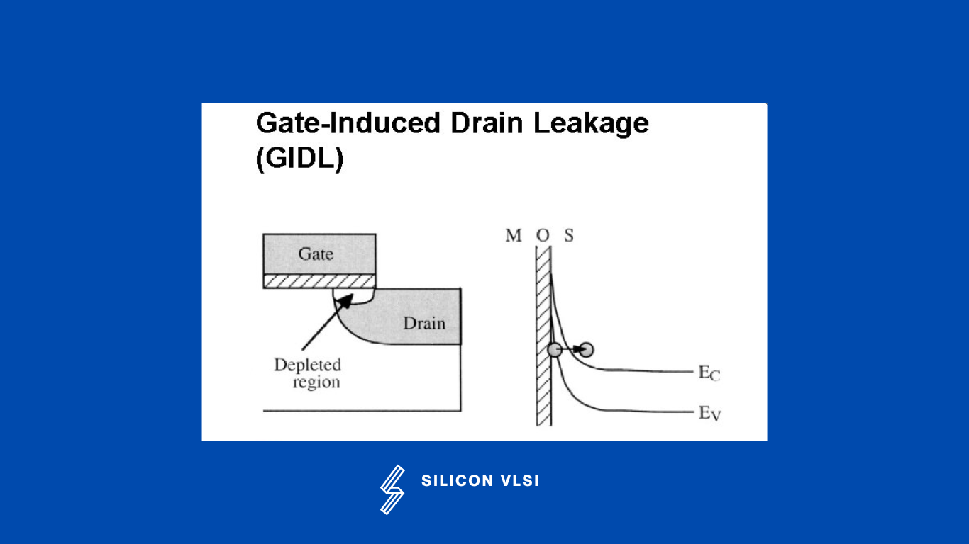
GIDL is a phenomenon that occurs when a high voltage is applied to the drain with the gate grounded, as a result, a deep-depletion region is formed underneath the gate-to-drain overlap region shown in Figure.
By tunneling valence band electrons into the conduction band, electron-hole pairs are created, which are then gathered by the drain and substrate.
The band-to-band tunneling process in silicon’s gate-to-drain overlap region is what causes gate-induced drain leakage current. The deep-depletion zone is always present and the band-to-band tunneling process can continue without forming an inversion layer because all the minority carriers produced thermally or by band-to-band tunneling in the drain region pass to the substrate due to the lateral field.
With rising VD and falling VG, this drain leakage current rises and appears to be independent of channel length.