

Advantages of FinFET Over Planar CMOS: 5 Essential Benefits
FinFET, or Fin Field-Effect Transistor, is a three-dimensional transistor architecture developed to overcome some of the scaling and leakage challenges of traditional planar CMOS.
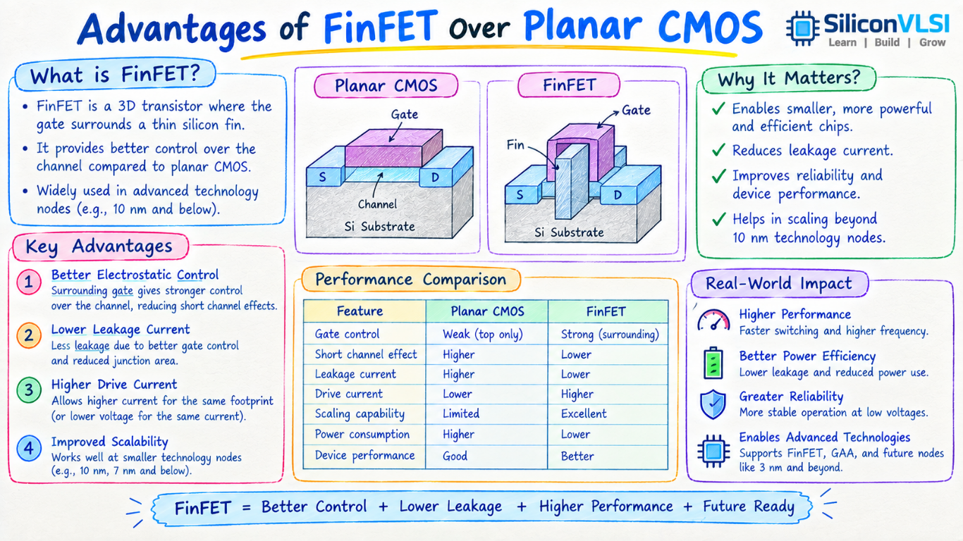
In a planar MOSFET, the gate controls the channel mainly from the top. In a FinFET, the channel is formed in a thin vertical silicon fin, and the gate surrounds multiple sides of the fin. This provides stronger electrostatic control of the channel.
As transistor dimensions become smaller, this improved control helps reduce several short-channel effects and enables better performance and power efficiency.
What Is FinFET?
A FinFET is a transistor in which the conducting channel is formed in a raised, fin-shaped semiconductor structure.
The gate is positioned around multiple sides of the fin, giving it better control over the channel compared with a conventional planar transistor.
A simplified comparison is:
Planar CMOS: Gate → controls channel mainly from one side
FinFET: Gate → controls channel from multiple sides
This stronger gate control is one of the main reasons FinFET technology became important for advanced CMOS scaling.
1. Better Short-Channel Control
One of the biggest advantages of FinFET over planar CMOS is improved short-channel control.
As the channel length becomes smaller, the drain can have a greater influence on the channel potential. This can lead to short-channel effects such as:
- Drain-Induced Barrier Lowering (DIBL)
- Threshold-voltage roll-off
- Increased subthreshold leakage
- Reduced control of the channel by the gate
Because the FinFET gate surrounds multiple sides of the channel, it provides stronger electrostatic control.
This helps suppress short-channel effects compared with a similarly scaled planar transistor.
2. Reduced Leakage Current
FinFETs can achieve lower off-state leakage than comparable planar CMOS devices because of their improved electrostatic control.
Better control of the channel helps reduce unwanted current when the transistor is supposed to be OFF.
This is particularly important because leakage becomes increasingly significant as transistor dimensions and supply voltages are scaled.
However, it is better to avoid describing every FinFET as simply a double-gate transistor. FinFETs commonly use a gate that controls multiple surfaces of the fin, often described as a tri-gate or multi-gate structure, depending on the implementation.
Reduced leakage can help improve overall power efficiency, especially in circuits containing a very large number of transistors.
3. Improved Power Efficiency
FinFET technology can provide a useful combination of performance and power efficiency.
Better electrostatic control allows designers to maintain transistor performance while controlling leakage and operating voltage.
CMOS dynamic power can be approximated by:
Pdynamic = α × C × VDD² × f
where:
- α = switching activity
- C = effective switched capacitance
- VDD = supply voltage
- f = operating frequency
Because power depends strongly on the square of the supply voltage, voltage scaling can provide significant power savings.
However, FinFET itself does not automatically mean that every design can operate at an arbitrarily lower voltage. The achievable operating voltage depends on the process technology, transistor characteristics, circuit requirements, timing, and reliability constraints.
4. Higher Performance
FinFETs can provide better performance than planar CMOS at advanced technology nodes because of their improved channel control.
Better electrostatic control can help designers achieve a useful combination of:
- Higher drive current
- Lower leakage
- Faster switching
- Better control of threshold voltage
- Improved performance at scaled dimensions
The actual performance advantage depends on the specific process technology and circuit design. Factors such as fin dimensions, gate length, parasitic capacitance, resistance, and interconnect delay also affect overall circuit speed.
Therefore, it is more accurate to say that FinFET enables better performance scaling rather than claiming that every FinFET is inherently faster than every planar transistor.
5. Better Scaling for Advanced CMOS
Traditional planar CMOS becomes increasingly difficult to scale because the gate loses electrostatic control over the channel as dimensions shrink.
FinFET addresses this problem by using a three-dimensional channel structure.
The gate controls the channel from multiple sides, which improves electrostatic control and makes the architecture more suitable for advanced technology nodes.
The basic idea is:
Smaller dimensions → stronger short-channel effects → weaker planar gate control
FinFET provides:
3D channel + multi-sided gate control → better electrostatic control → improved scaling
This architecture therefore played an important role in extending CMOS scaling beyond the practical limits of traditional planar transistor structures.
FinFET vs Planar CMOS
| Feature | Planar CMOS | FinFET |
|---|---|---|
| Channel structure | Planar | 3D fin |
| Gate control | Mainly from the top | Multiple sides of the fin |
| Short-channel control | More difficult at very small dimensions | Better |
| Leakage control | Becomes challenging with scaling | Generally improved |
| Scaling capability | Limited at advanced dimensions | Better suited to advanced nodes |
| Drive current control | Based largely on planar device width | Strongly influenced by fin geometry and number of fins |
| Layout | Relatively simple | More constrained by fin-based design |
| Manufacturing | Mature and comparatively simpler | More complex 3D process |
Why FinFET Is Important in VLSI
FinFET technology changed the way advanced CMOS transistors are designed.
In planar CMOS, simply reducing the transistor dimensions eventually causes problems with leakage and electrostatic control. FinFET introduces a three-dimensional structure to improve gate control without relying solely on reducing the planar channel dimensions.
This makes FinFET particularly useful for high-density digital circuits such as:
- CPUs
- GPUs
- Mobile processors
- SRAM
- SoCs
- High-performance digital ICs
Fin-based transistor architectures have also influenced the development of newer transistor structures such as gate-all-around (GAA) devices, where the gate provides even more complete control around the channel.
Key Takeaways
The main advantages of FinFET over planar CMOS are:
- Better short-channel control due to multi-sided gate control.
- Lower leakage through improved electrostatic control.
- Better power efficiency and greater flexibility for voltage scaling.
- Higher performance potential at advanced technology nodes.
- Improved scalability compared with conventional planar MOSFETs.
Frequently Asked Questions
What is the main advantage of FinFET over planar CMOS?
The main advantage is improved electrostatic control of the channel. The gate surrounds multiple sides of the fin, helping control short-channel effects as transistor dimensions shrink.
Does FinFET completely eliminate leakage current?
No. FinFETs reduce leakage compared with comparable planar architectures, but leakage current still exists and depends on the process, device dimensions, temperature, threshold voltage, and operating conditions.
Is FinFET a double-gate transistor?
FinFETs are generally described as multi-gate transistors because the gate can control multiple surfaces of the fin. Specific implementations may have different gate geometries, so calling all FinFETs simply “double-gate” is an oversimplification.
Why is FinFET better for scaling?
The three-dimensional fin and multi-sided gate provide stronger control over the channel. This helps reduce short-channel effects that become increasingly difficult to control in scaled planar MOSFETs.
What comes after FinFET?
Gate-all-around (GAA) transistor architectures are a major successor to FinFET in advanced CMOS. In a GAA device, the gate surrounds the channel more completely, providing stronger electrostatic control.
Conclusion
The advantages of FinFET over planar CMOS mainly come from its three-dimensional transistor structure and improved gate control.
By controlling the channel from multiple sides, FinFETs can provide better short-channel behavior, lower leakage, improved performance and better scaling capability than conventional planar CMOS at advanced technology nodes.
FinFET technology therefore represents an important step in the evolution of CMOS technology and provides the foundation for understanding newer transistor architectures such as GAA.