
What Is The Antenna Effect in VLSI?
During the Fabrication Process, a large amount of charge is induced in plasma etching, ion implantation, and other processes(CMP). If a large interconnect is directly connected to the Gate of a MOSFET, then this larger conducting material will act as an Antenna and will receive the induced charge of the Fabrication Process. The charge due to these extra carriers might be too much for the thin gate to handle, and it may also damage the thin oxide layer. So, the Antenna effect may result in the breakdown of Gate Oxide or degrade the I-V Characteristics.
The antenna effect in VLSI, also known as plasma-induced gate-oxide damage or plasma-induced damage, is a phenomenon where a large amount of charge is induced during plasma etching and other procedures. In VLSI, the term “antenna effect” specifically refers to the charge collecting effect, rather than referring to an actual antenna device.
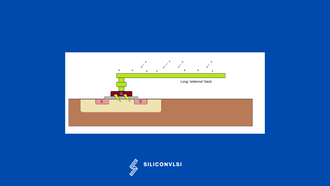
During the fabrication process, we need to etch out the unwanted oxide layer from the wafer, which can be done using plasma etching. Plasma contains highly energetic ions and radicals for etching that get collected by interconnect. The amount of charge accumulation depends on the surface area of the interconnects area. These collected ions increase the potential of interconnects and if the interconnect is connected to the gate, it may lead to permanent damage to the device gate oxide.
Process Induced Damage(PID) degradation effects
Increase of gate oxide leakage current.
Increase of hot-electron effects.
Increase of the threshold voltage
Degradation of the gate oxide lifetime.
Antenna rules:
The antenna rule is provided by Foundry which must be followed during the layout design. In the antenna rules, the most common rule is the Antenna Ratio, Metal area ratio, and via area ratio.
Antenna area/gate area < Maximum Antenna Ratio
- Metal area antenna rule: The maximum limit to the ratio of the metal line area to the connected gates area.
- Via or contact area: The maximum limit to the ratio of the via or contact area to the connected gates area.
Antenna Effect Prevention Techniques
Insert Jumper
To prevent the antenna effect from destroying your circuit you need to reduce the floating metal/gate area ratio or give the charge a safe way to dissipate to the ground before it can build up and cause damage. To reduce the floating metal/gate area ratio, the layout designer must change the routing and go for the higher metal. Long metal can be taken to a higher metal routing layer. This is known as metal jumping. This metal jumping is usually done near the gate.
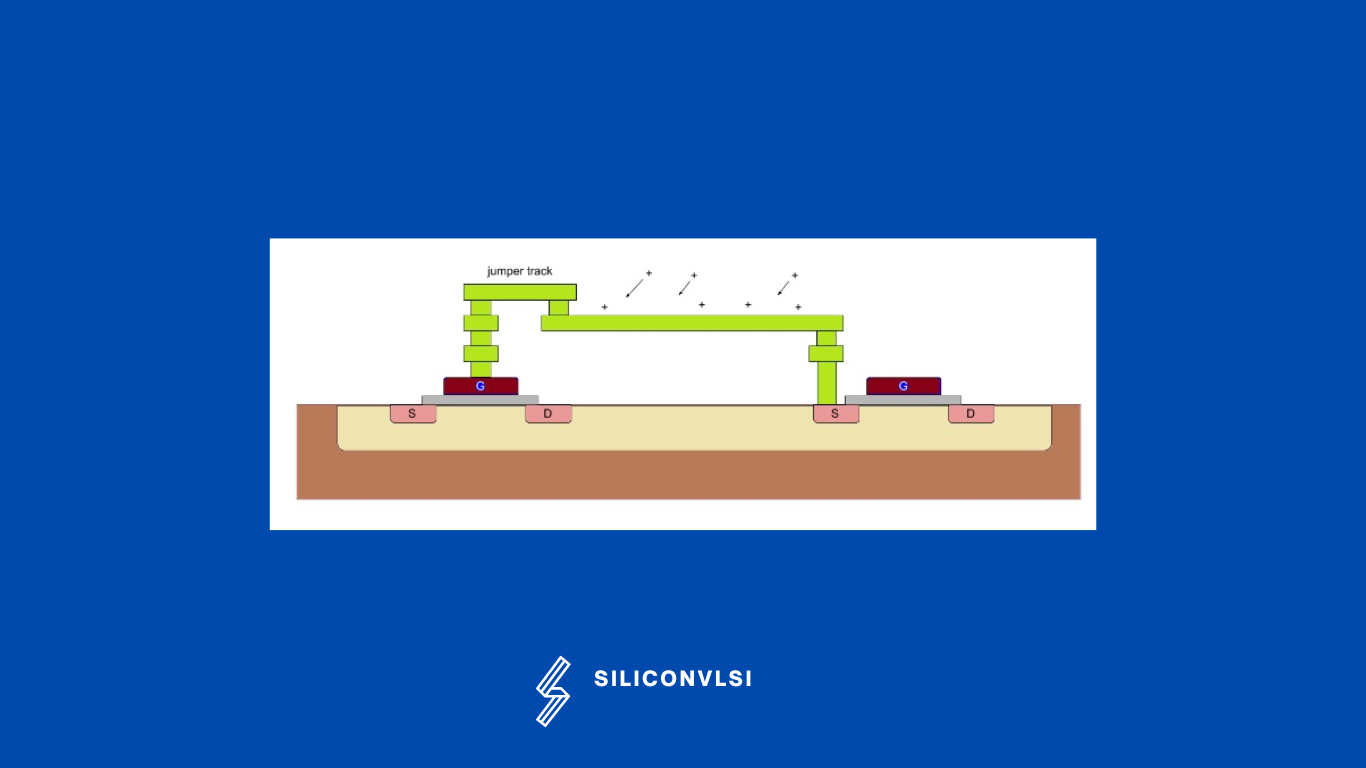
This metal jumping will break the long interconnect and hence the charge collected on the long interconnect will not discharge through gate oxide because the higher metal layer is not yet fabricated. Why do we go for the highest metal jumper because lower metal is already fabricated during the fabrication process, so the overall area will remain the same, so do we need to go for the higher metal jumper? Jumpers can be used to effectively control antenna issues, but complicate the routing by adding lots of extra vias and small pieces of wire into the layout.
Diode Insertion
The diode helps dissipate charges accumulated on metal. The diode should be placed as near as possible to the gate of the device on the low level of metal. Connecting a diode to the gate electrode provides a discharging path for the static charge present on the metal layer. The diode should always be connected in reverse bias, with the cathode connected to the gate electrode and the anode connected to ground potential, so that in normal operation diode act as a reverse bias, and during fabrication, it will act as a restore.
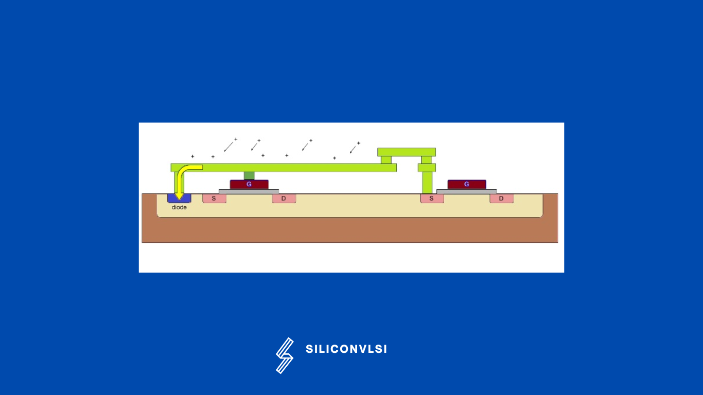
Diodes are a very effective way of preventing antenna effect damage, but the disadvantage of inserting diodes into a circuit is that they add extra capacitance, which affects circuit performance, and they increase area.
Where these charges will go from the Antenna diode?
Charges that accumulate on metal structures in an integrated circuit and are discharged through an antenna diode typically flow through the diode to a safe place, preventing damage. This safe place can be one of the following:
Ground or Power Grid: The charges go to the circuit’s ground or power grid, which safely absorbs them.
Local Discharge: Antenna diodes are placed close to the metal structures, so charges are discharged nearby, reducing the risk of damage.
Diode Substrate Connection: Some diodes are linked to the circuit’s substrate, providing a safe path for the charges.
External Circuitry: In complex circuits, the charges may be directed to external components designed for safe discharge.
Reduce the via-area
Large via area also results in process antenna violation. Large multiple via also may cause the Antenna effect. While conversion of multi-cut vias to double-cut via or double-cut vias to single-cut via reducing the cut area. This may impose serious reliability issues such as electromigration.
What Causes Antenna Effect During Fabrication?
- Plasma etching
- Charge accumulation
- Gate oxide damage
Antenna Rules in VLSI
- Antenna ratio
- Metal area to gate area ratio
- Foundry limits
Related VLSI Topics
DRC (Design Rule Check)
DRC is a physical verification process used to ensure that the layout follows all foundry manufacturing rules. It helps identify violations such as minimum spacing errors, width violations, enclosure violations, density violations, and antenna violations before tapeout.
👉 Read More: https://siliconvlsi.com/drc/
LVS (Layout Versus Schematic)
LVS verifies whether the physical layout matches the intended schematic design. It is one of the most important signoff verification checks used to detect missing devices, shorts, opens, and connectivity mismatches.
👉 Read More: https://siliconvlsi.com/lvs/
Physical Verification in VLSI
Physical verification is a signoff process that ensures the layout is manufacturable and functionally correct. It includes DRC, LVS, ERC, antenna checks, density checks, and several advanced verification methodologies used in modern semiconductor design.
👉 Read More: https://siliconvlsi.com/physical-verification/
Frequently Asked Questions (FAQs)
What is the antenna effect in VLSI?
The antenna effect is a phenomenon where charge accumulates on metal interconnects during fabrication and damages the gate oxide of MOS transistors.
Why is the antenna effect harmful?
Excessive charge accumulation can break down the gate oxide, increase leakage current, and degrade transistor reliability.
How can antenna violations be fixed?
Antenna violations can be fixed using antenna diodes, metal jumping, layer hopping, routing modifications, and foundry-approved antenna solutions.
What is an antenna diode?
An antenna diode provides a discharge path for accumulated charge during fabrication, preventing damage to gate oxide.
What is antenna ratio?
Antenna ratio is the ratio of metal area to gate area. Foundries specify maximum allowable antenna ratios for each process technology.