
Flip chip and Wire bond
Generally, flip chip and wire bond are used for connection between the chip and circuit board. Both have their own advantage and disadvantage. According to the application, flip chip and wire bond may use. In the wire bond method, the die faces up and is attached to the package via wires. while in flip chip faces down and is typically attached via solder bumps similar to ones that attach BGA packages to the printed circuit board. Let’s try to understand both terms separately first,
What is a flip chip?
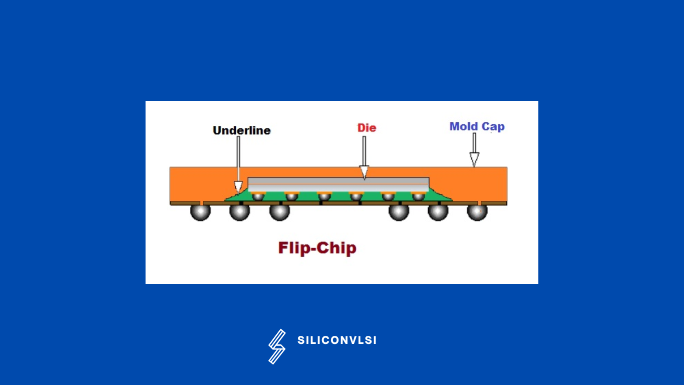
Flip chip means “flipped over the circuit board” facing downward. Instead of facing the upside. So flip chip allows for a large number of interconnects with shorter distances than wire, which greatly reduces the distance and area. The process of attaching a semiconductor die to a substrate or carrier with the bond pad facing down is referred to as a flip chip.
On the die bond pad, there is a conductive bump that is used to make the electrical connection. The stand-off space between the die and substrate is normally filled with a non-conductive adhesive known as underfill once the die is connected. Between the die and carrier, the underfill relieves tension, increases robustness, and shields the component from any moisture infiltration.
Comparing flip-chip bonding to other connectivity techniques can provide a variety of benefits. Since the entire region of the die can be used for connections, flip chip bonding can increase the number of I/Os. The speed of a device can be increased since the connectivity paths are shorter than they would be with wire bonds. Additionally, the removal of wire bond loops results in a reduced form factor.
Flip chip Process Advantage
- Reliability
- High I/O density.
- Small package size.
- Less Power consumption.
- Lower stress on a given area.
- Better electrical performance.
- Better heat dissipation performance.
- More stable structural characteristics.
- Require simpler processing equipment.
- Flip-chip can achieve high yields and reliability
Flip chip Process Disadvantage
- High price
- Flipchip Process needs to design the RDL layer as the top layer, The production, and processing of the RDL require an additional process and are costly.
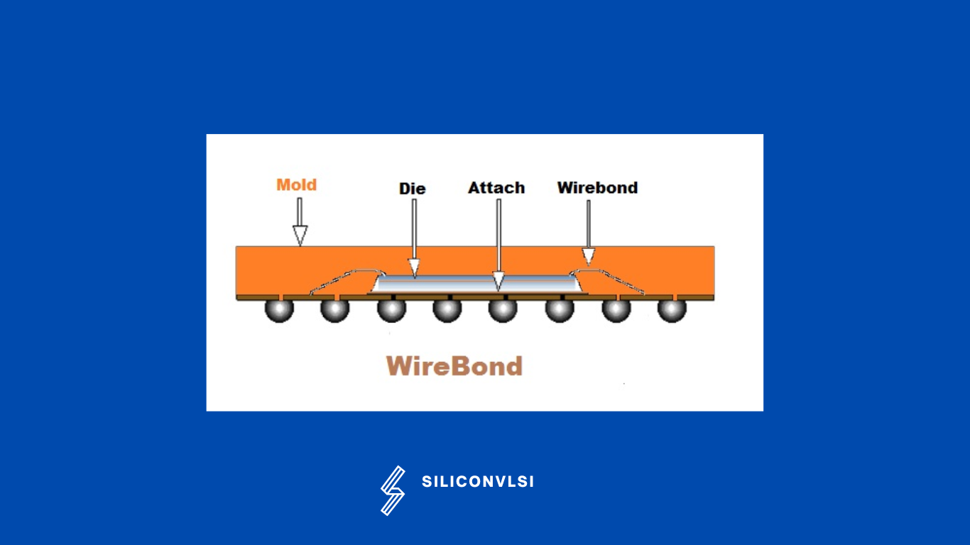
What is Wire Bond
To create an electrical connection in circuits, wire bonding is mostly employed in the microelectronics sector of the electronics industry. In order to mount the die onto the substrate, such as a lead frame or multilayer substrate, wire bonding always needs to come first. The two most common processes used for wire bonding are gold ball bonding and aluminum wedge bonding.
Wire bonding Advantages
- Production cost is very less
- Reliability is more in wire bond
- Testing for connection is very simple
- Require less temperature during the process
- Handling is very simple for complex circuits.
- More flexibility in chip, package, and substrate geometry
Wire bonding Disadvantages
- The large footprint is require
- Slower interconnection rate
- Interconnection length is required large
- Create a vibration of the substrate during the process
Comparison between the flip chip and wire bond
| Parameter | Wire Bond | Flip chip |
| Pin connection | Provide less I/O count | Provide a higher I/O count |
| Interconnections path | Long | Short |
| Interconnection material | Gold | Solder balls |
| Reliability |
Higher
|
Lower
|
|
Thermal dissipation efficiency
|
Lower
|
Higher
|
|
Cost
|
Less expensive process
|
Expensive process
|
What is major advantage of using flip chip over wire bond package?
Flip chips are recognized for offering numerous advantages over traditional wire-bond packaging, such as superior thermal and electrical performance, high I/O capability, substrate flexibility to meet diverse performance needs, established process equipment expertise, proven construction, and smaller form factors, they have not emerged as a cost-effective packaging solution.