
For any given transistor, we need to think about power, performance, and Area(PPA), Let’s try to understand FD-SOI and FinFET.
What is a FinFET?
FinFET is a regular transistor flipped on its side. We took the standard, flat MOSFET and made it 3D. This dramatically increases the surface area of the gate on the channel, reducing leakage. We called it FinFET because its shape is like FIN types.

It turns out that these transistors operate admirably and can push a significant amount of current. It just so happens that they are quite pricey since they are difficult to make. Not all devices can afford Finfets, but they still require better transistors than what 28nm and older can offer. These transistors are fantastic for things like CPUs, GPUs, mobile Socs, etc., but they are not well suited for things like IoT, for instance.
FinFET-Benefits
- Need lower supply voltage.
- Less Sub-threshold Leakage.
- It can achieve higher frequency numbers.
- Reduced power consumption compared to planar transistors.
FinFET -Drawback
- Width Quantized.
- Difficult to control dynamic Vth.
- Higher parasitics due to Three side control.
- Very high capacitances due to fins.
- Corner effect.
- Fabrication Cost.
What is FD-SOI
FD-SOI means Fully Depleted Silicon On Insulator, is a planar process technology that relies on an ultra-thin layer of insulator, called the buried oxide, positioned on top of the base silicon.
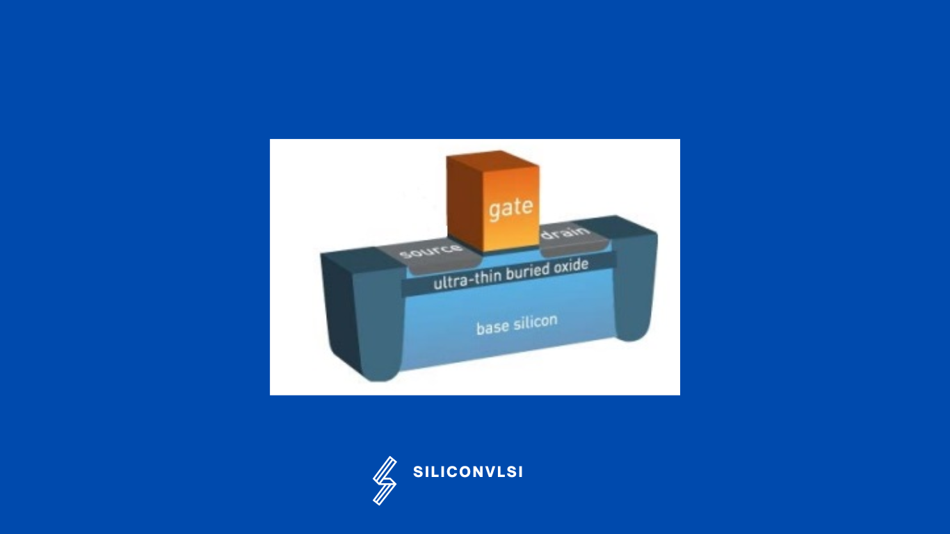
Compared to traditional bulk technology, FD-design SOIs provide significantly superior transistor electrostatic properties. The parasitic capacitance between the source and the drain is reduced by the buried oxide layer. Additionally, it effectively limits the flow of electrons from the source to the drain, thereby lowering leakage currents that impair performance.
FD-SOI Advantages
- Excellent VT control
- We can give body Bias
- Limited Short Channel Effects
- Very good Sub-threshold Slope
- Low DIBL (Drain Induced Barrier Lowering)
- Excellent electrostatic control of the channel
- Minimum junction capacitance and diode leakage
FD-SOI Disadvantages
- Complex Fabrication
- Wafer suppliers are limited for FD-SOI
- Multi- VT more complex to implement
What is the difference between SOI and FD-SOI?
FD-SOI, or Fully Depleted Silicon-On-Insulator, employs an extremely thin layer of silicon on top of a buried oxide layer. This design is aimed at minimizing leakage and variation in semiconductor chips. Additionally, FD-SOI incorporates a back-bias feature, which further enhances its performance characteristics.
The broader category of Silicon-On-Insulator (SOI) technology involves the use of a layered SOI substrate instead of the traditional bulk substrate in semiconductor fabrication processes. This layered substrate configuration helps in reducing parasitic capacitance, improving device isolation, and enhancing overall chip performance.