
Hot Electron effect
When Vds is high, the electron near the gate will receive high kinetic energy, and some of these electrons might be trapped in gate oxide, which may damage the gate oxide or change Vt(threshold voltage). This is called a “Hot Electron Effect.” This leads to the deposition of negative charge on the gate which leads to an increase in threshold voltage by increasing flat band voltage. In addition, these hot carriers can rupture stable Si-H bonds creating fast interface states that degrade MOSFET parameters such as gain.
A hot electron effect was observed in short channel MOSFET due to the presence of the high lateral and transverse electric field. The problem of hot electrons has increased as technologies scale down because device features have scaled proportionally faster than voltage. This leads to the devices having higher field strengths and thinner gate oxides. So there might be higher chances for this effect.
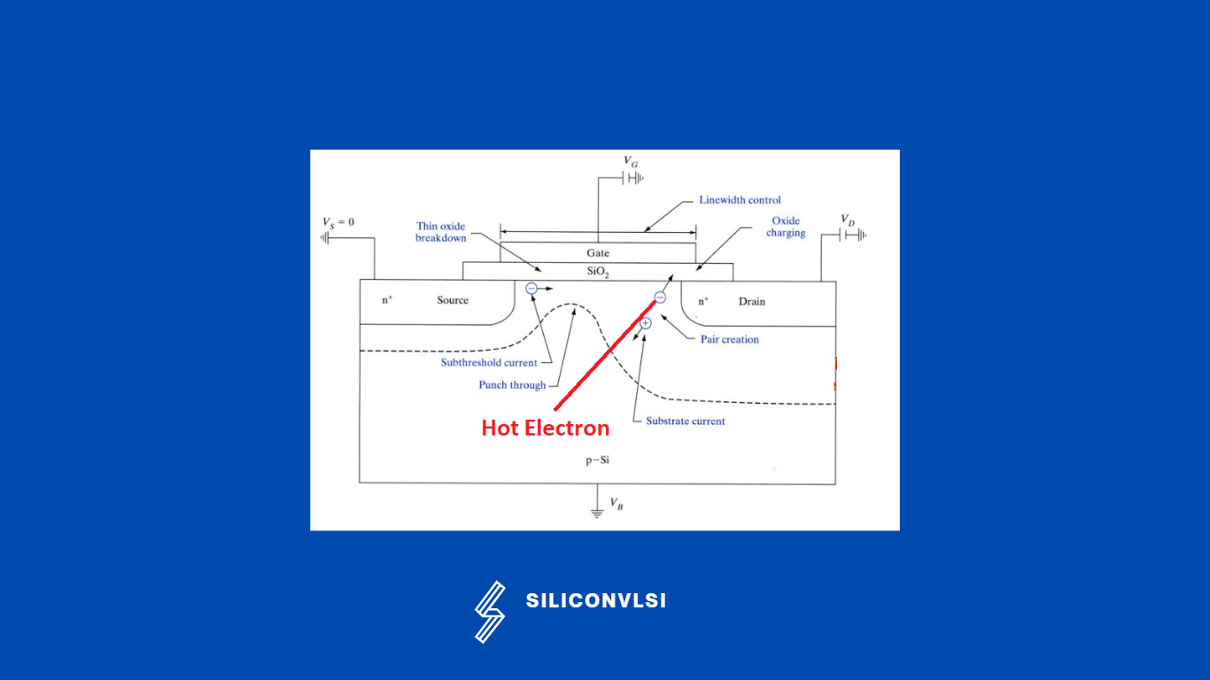
The resulting bulk minority carriers can either be injected into the gate oxide or collected by the drain. The bulk current produced by the majority of carriers generated can be used to measure the degree of impact ionization. The hot carrier degrading effect is caused by the injection of carriers into the gate oxide.
Effect on Transistor.
At the silicon-oxide interface, the trap can also be operated by hot electrons. As a result, the transistor’s lifetime is limited by this effect. As a result, the electric field in the pinch-off region plays a key role in determining the hot carriers‘ energy. It is considered as an aging effect in VLSI design.
How can we stop the hot electron effect?
- Reduce the supply voltage.
- Use a long-channel device.
- Use STI(Shallow trench isolation).
- Hot carrier effects are less problematic for holes in p-MOSFETs
- LDD (lightly doped drain) can be a solution for the stress of the hot carrier effect.