
Cross talk in Digital Circuit
Cross talk, a proportional noise source in digital circuits, poses a challenge that cannot be easily addressed by simply scaling signal levels. Instead, controlling circuit geometry and adopting specific signaling conventions are crucial for minimizing cross-talk. Here are some key strategies to mitigate cross-talk:
Circuit Geometry: Avoid allowing the capacitance between two signal wires to become too large. Running two wires on the same layer in parallel for an extended distance should be avoided. Wires on adjacent layers should run perpendicular to each other, reducing the likelihood of coupling.
Floating Nodes: Whenever possible, avoid floating nodes, especially in sensitive areas prone to cross-talk issues. Nodes like precharged buses should be equipped with keeper devices to lower their impedance and reduce vulnerability to interference.
Signal Separation: Keep sensitive nodes well-separated from full-swing signals to minimize the risk of cross-talk affecting critical areas of the circuit.
Rise and Fall Times: Maximize the rise and fall times of signals, taking into account timing constraints. Slower transitions can reduce the energy coupled into neighboring wires.
Differential Signaling: Implement differential signaling in sensitive low-swing wiring networks. This approach transforms cross-talk signals into common-mode noise sources, which do not disrupt the circuit’s operation.
Shielding: When necessary, introduce a shielding wire, either GND or VDD, between the two signals. This configuration effectively converts the interwire capacitance into capacitance-to-ground, eliminating interference
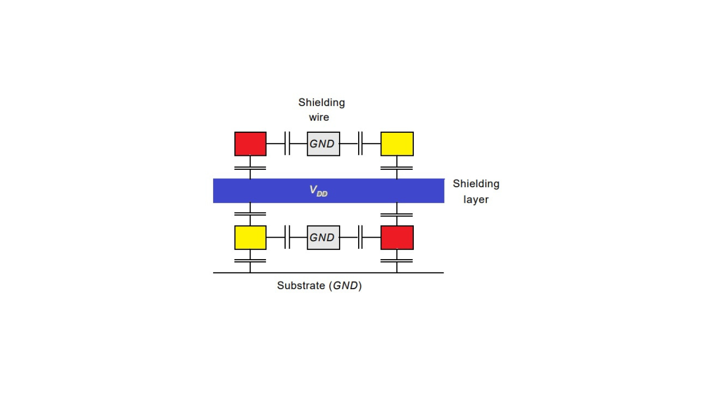
Furthermore, to decrease the interwire capacitance between signals on different layers, additional routing layers can be introduced. In this approach, each signal layer is interleaved with a metal plane connected to GND or VDD. This design helps reduce cross talk by effectively isolating signal layers from each other.
Why is it not advisable to have two wires on the same layer run parallel for a long distance?
Running two wires on the same layer in parallel for an extended distance is not advisable because it can lead to increased capacitance between the wires, resulting in higher cross-talk. To minimize cross-talk, it’s better to run wires on adjacent layers perpendicular to each other.
How can you reduce the sensitivity to cross-talk in nodes, such as precharged buses?
To reduce the sensitivity to cross-talk in nodes like precharged buses, you can equip them with keeper devices. These keeper devices help reduce impedance and minimize the impact of cross-talk.
What’s the advantage of using differential signaling in sensitive low-swing wiring networks?
Using differential signaling in sensitive low-swing wiring networks helps mitigate the impact of cross-talk. It converts the cross-talk signal into a common-mode noise source that doesn’t affect the circuit’s operation, thereby improving signal integrity.
What role does adding a shielding wire (GND or VDD) between two signals play in reducing interference?
Adding a shielding wire (GND or VDD) between two signals effectively transforms the interwire capacitance into a capacitance to the ground. This configuration helps eliminate interference between the signals, reducing cross-talk.
How can the interwire capacitance between signals on different layers be reduced further?
To further reduce the interwire capacitance between signals on different layers, you can add extra routing layers. When four or more routing layers are available, you can employ an approach commonly used in printed circuit board design, where each signal layer is interleaved with a GND or VDD metal plane. This reduces capacitance and minimizes cross-talk.