
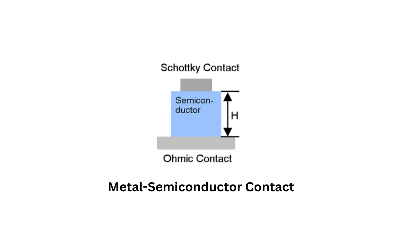
Metal-Semiconductor Ohmic Contact
By heavily doping the semiconductor at the interface with the metal, the depletion zone can be made very small, allowing charge carriers to “tunnel through” the barrier. This phenomenon is a quantum-physical effect, and it ensures that the diode can conduct current effectively.
Besides the Schottky diode effect, there are several other physical interactions between the semiconductor and metal materials. To prevent undesirable effects, additional process steps may be necessary, depending on the specific processes and materials used in the fabrication.
The Importance of Doping in the Silicon-Metal Contact Area
In the layout design, a key aspect is ensuring that the contact area in the silicon is heavily doped. This high doping level ensures a linear current-voltage response at the silicon-metal interface, leading to the desired “ohmic” contact response. An ohmic contact means that the current passing through the contact is directly proportional to the voltage applied. This linear behavior is important for reliable and predictable electronic device performance.
An ohmic contact means that the current passing through the contact is directly proportional to the voltage applied.
The typical resistance values for single contacts are in the single to double-digit ohm range. Low-resistance contacts are essential for minimizing power losses and achieving efficient electronic device operation.
In conclusion, the interaction between the semiconductor and metal materials at their interface has significant implications for the device’s behavior, including the formation of a depletion zone and the Schottky diode effect. Properly doping the silicon-metal contact area ensures an ohmic contact response, leading to linear current-voltage characteristics and optimized electronic device performance