Understanding MOSFETs – Metal Oxide Silicon Field Effect Transistors
MOSFETs are a Metal Oxide Silicon Field Effect Transistor.MOSFETs are electronic devices used to switch or amplify voltages in circuits. It is a voltage-controlled device and is constructed by three terminals. The terminals of MOSFET are named as follows,
- Source
- Drain
- Gate
- Body
MOS Capacitor
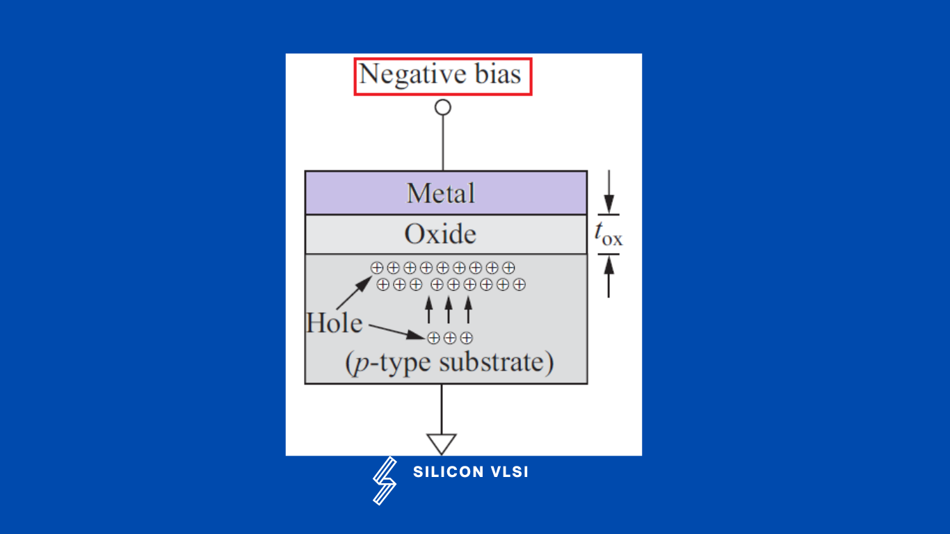
In a MOS capacitor, the lower plate is replaced by a semiconductor material which is often called the substrate. The structure of a MOS capacitor is shown in Figure 1. Let us consider that the substrate material is p-type. The p-type substrate has the majority of carrier holes distributed over the entire bulk material.
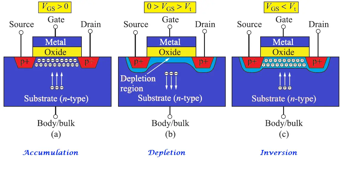
If the upper plate is negatively charged, holes will be attracted toward the upper plate and will accumulate near the oxide–semiconductor interface. This situation is the same as that of a parallel plate capacitor. This metal oxide semiconductor structure is known as a MOS capacitor. #
MOS capacitance Equation
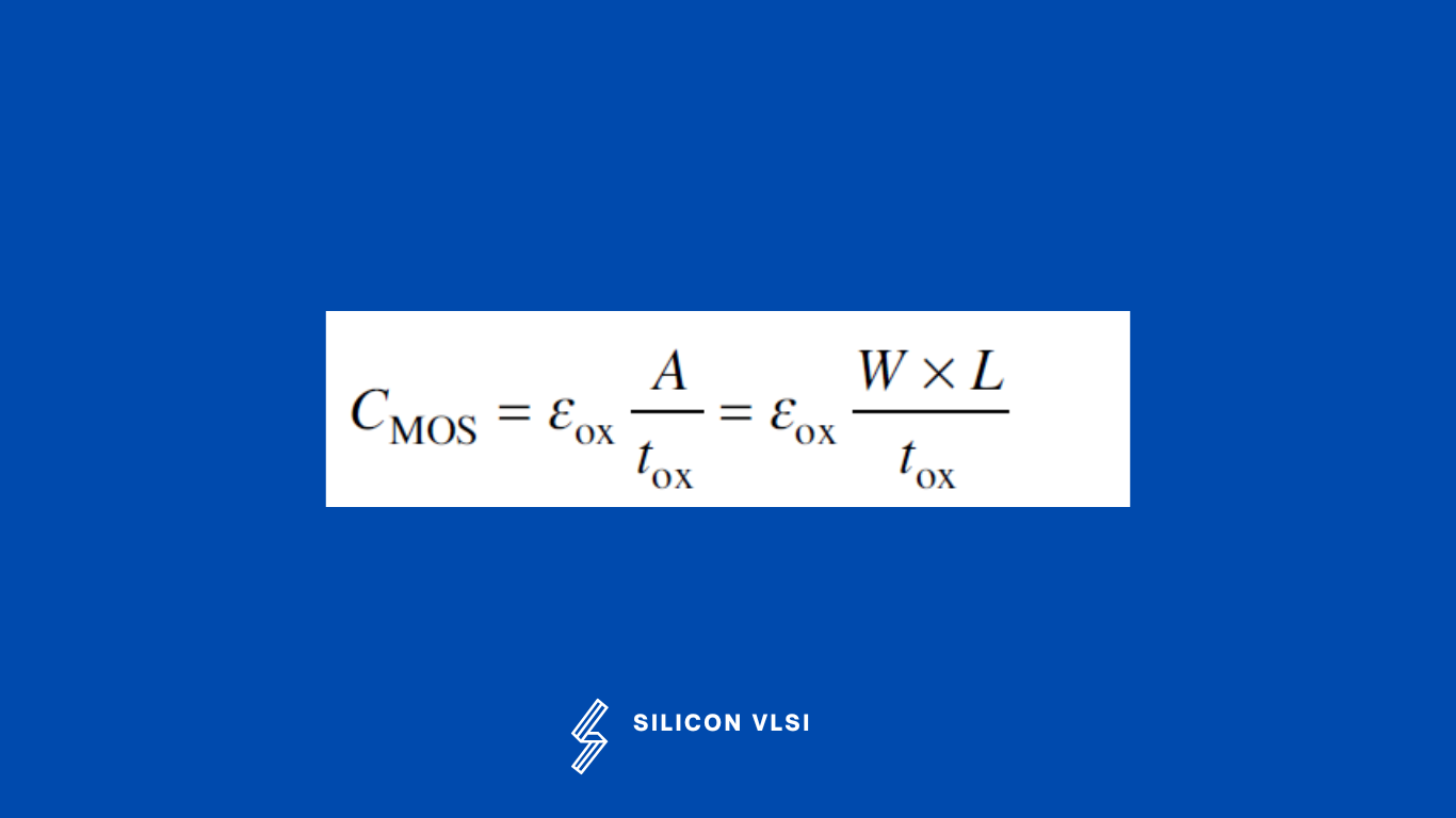
Where the area of the MOS capacitor is A = (W × L) and tox is the oxide thickness, and εox is the dielectric constant of the oxide material. Let us now understand the behavior of MOS capacitors under different bias conditions, by different modes of Operation. #
Modes of Operation of MOSFET
There are three modes of MOSFET, enhancement mode depletion mode, and inversion mode MOSFET. #
Enhancement Mode
First, we apply a negative voltage to the upper plate. The holes in the substrate will be attracted toward the oxide surface and they will accumulate underneath the oxide surface. This phenomenon is called accumulation. Hence, can get a capacitance which is given by the expression given in the above equation. #
Depletion Mode
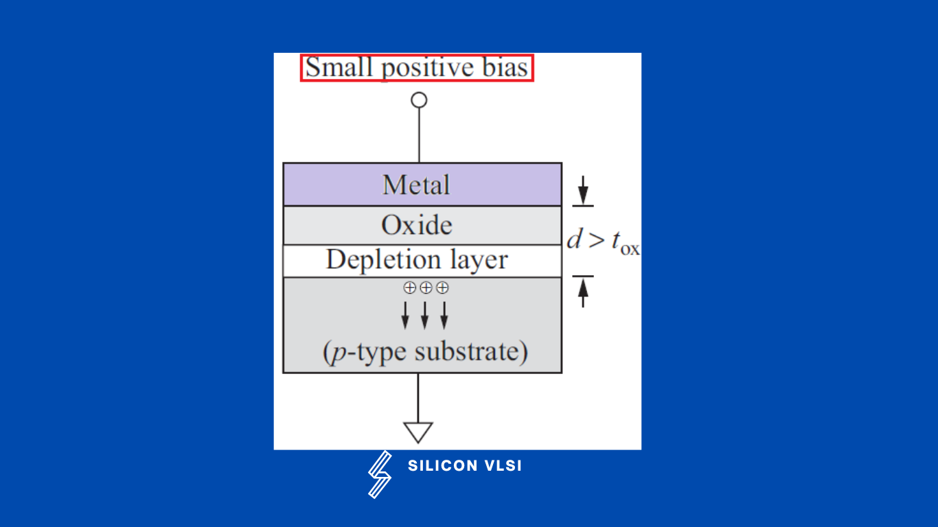
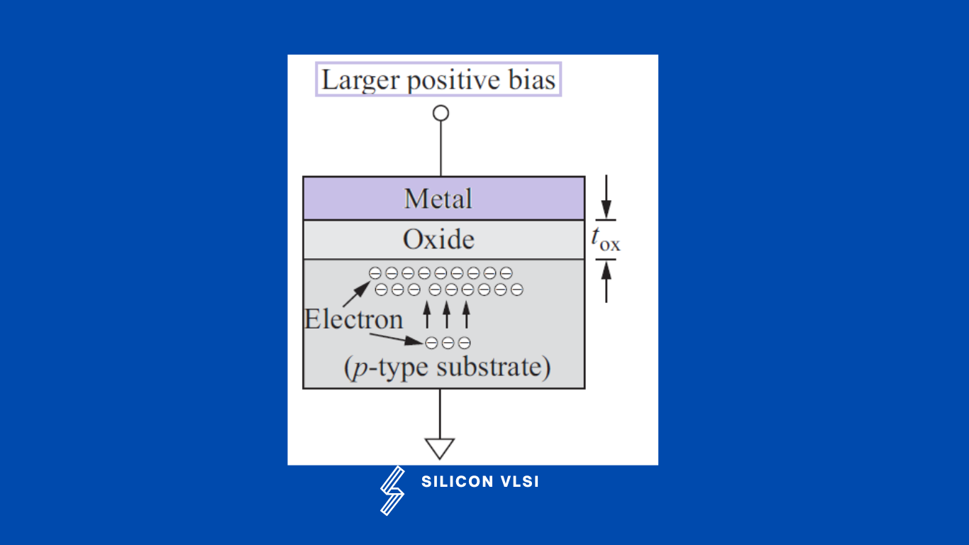
Now let’s apply a small positive voltage to the upper plate. In this case, the electrons will be attracted and the holes will be repelled. However, in a p-type semiconductor, there are very few electrons as compared to the holes. The negative charges are created by the ionized acceptors after the holes have been pushed out of them.
But the acceptors are fixed in their locations and cannot be driven to the edge of the insulator. Hence, there will be a depletion region created underneath the oxide layer. Therefore, the distance of the induced charge from the upper plate increases. As a result, the capacitance is lower as compared to the parallel plate capacitor. #
Inversion Mode
If a positive voltage is applied to the upper plate, the thickness of the depletion layer continues to increase. Thus, the capacitance continues to decrease. This does not, however, continue indefinitely. We know from the law of mass action that as hole density reduces, the electron density increases.
At some point, the hole density is reduced and electron density is increased to such an extent that electrons now become the majority carriers near the silicon dioxide interface. This phenomenon is known as Inversion Mode. #
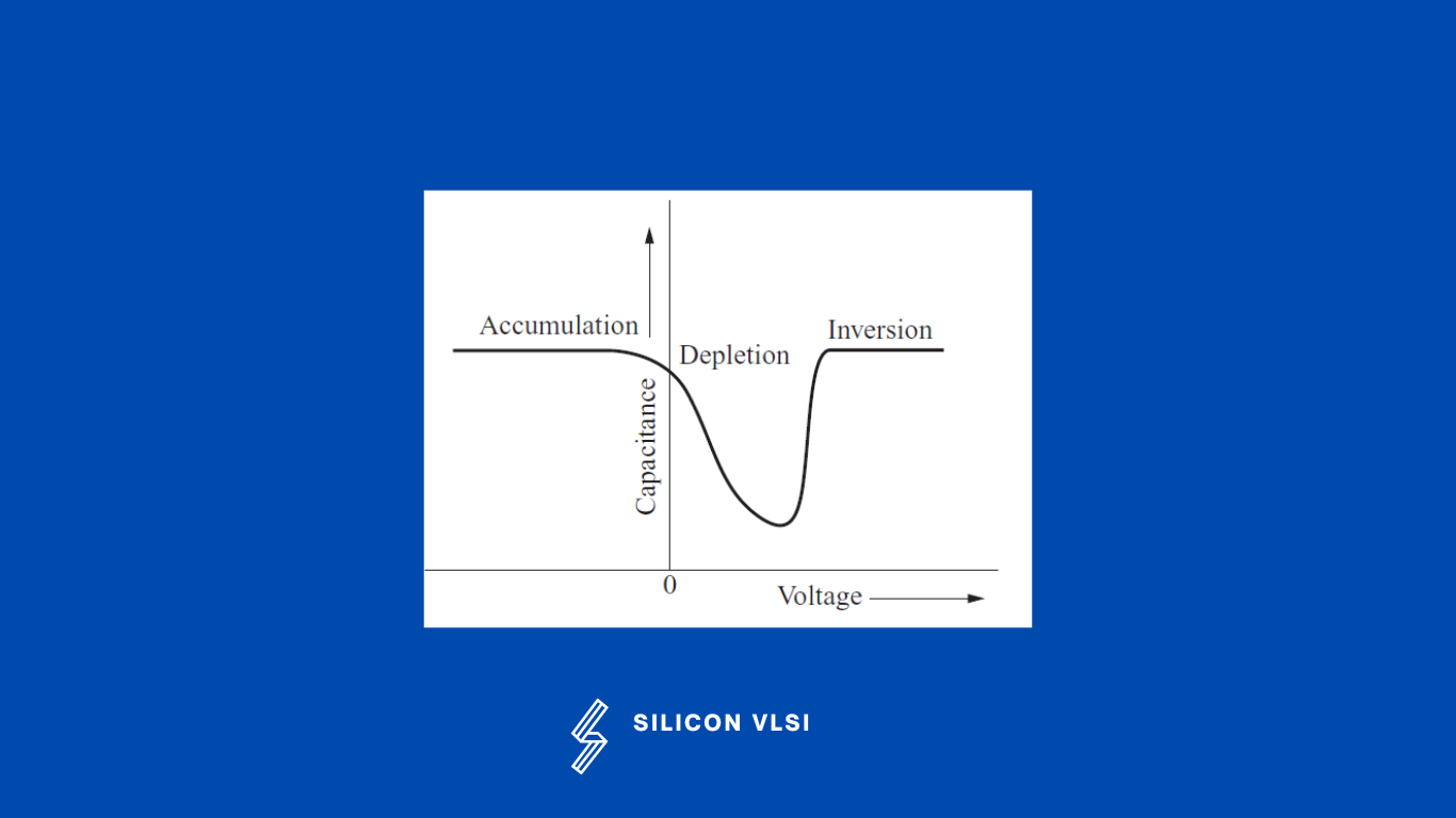
MOS capacitance-voltage characteristics
In short, for all, enhancement mode depletion mode, and inversion mode MOSFET, MOS capacitance-voltage characteristics are described in the following figure, #
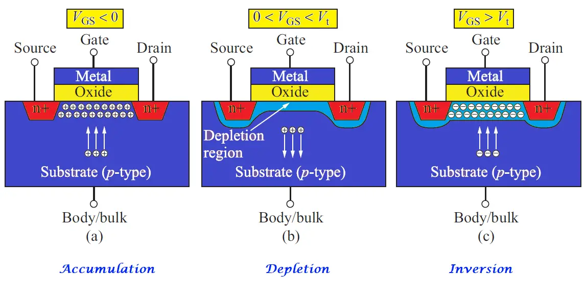
NMOS under different operating conditions
PMOS under different operating conditions