
Reverse Breakdown Characteristic
What is a Reverse Breakdown in VLSI?
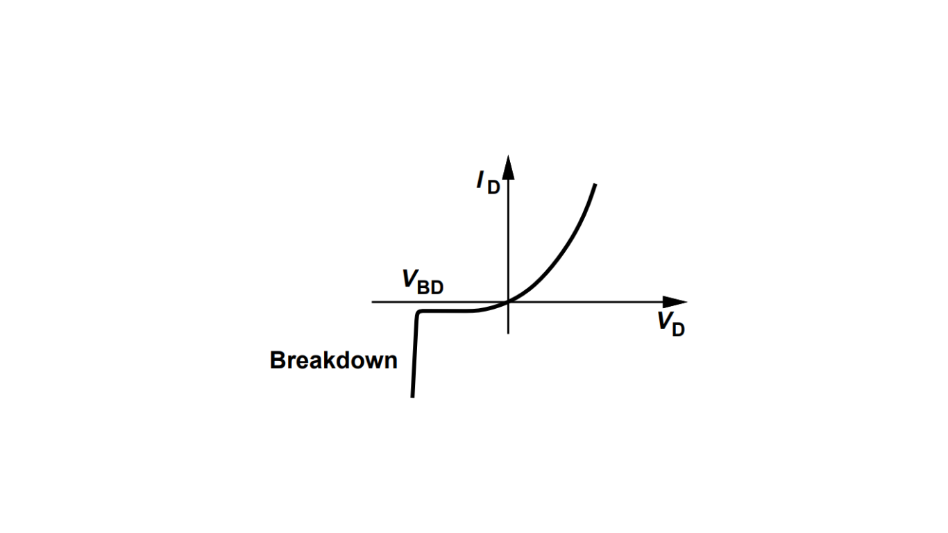
When you apply reverse bias to a pn junction, it carries only a small, relatively constant current. However, as the reverse voltage across the device increases, you’ll eventually see “breakdown” occur, leading to a sudden, enormous current. Figure 1 plots the device I/V characteristic, displaying this effect.
Understanding Breakdown
Breakdown due to high voltage and a high electric field can occur in any material. A well-known example of this is lightning, where the electric field in the air becomes so intense that it ionizes the oxygen molecules, lowering the air’s resistance and causing a tremendous current flow.
Breakdown Mechanisms in pn Junctions
In pn junctions, breakdown can occur through one of two possible mechanisms: the “Zener effect” and the “avalanche effect.”
Zener Effect: This mechanism occurs in heavily doped pn junctions. When the reverse voltage reaches a certain critical level, the strong electric field causes electrons to tunnel through the depletion region. This tunneling effect results in a significant increase in current.
Avalanche Effect: This mechanism occurs in lightly doped pn junctions. As the reverse voltage increases, the electric field accelerates charge carriers (electrons and holes), which gain enough energy to create additional charge carriers through collisions with the atoms in the depletion region. This multiplication effect leads to a rapid and massive increase in current.
Controlling Breakdown
Both the Zener effect and the avalanche effect can cause breakdown in pn junctions, depending on the specific characteristics of the junction and the applied voltage. Understanding and controlling these phenomena is essential for us to design and use semiconductor devices effectively and safely