
What is Temperature Inversion?
Temperature inversion is a phenomenon that occurs when the temperature of the channel region of a semiconductor device is higher than the temperature of the source and drain regions. This creates a high-density region of minority carriers in the channel, which can lead to various performance issues.
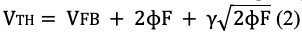
The definition of the threshold voltage is the minimum voltage required for the flow of electrons through the channel. it’s the value of the gate-source voltage when the conducting channel is just ready to connect to the source and drain contacts of the transistor.It is denoted by the VTH of a MOSFET.
At a high supply voltage, a higher temperature increases the delay. At a low supply voltage, a higher temperature decreases the delay. Thus, the delay increases or decreases with increasing temperature depending on the magnitude of the supply voltage (VDD).
Effect of temperature on mobility
As temperature increases, lattice vibrations increase, and the probability of an electron being scattered by the lattice increases. Thus, in high temperatures, mobility is limited by phonon scattering, causing mobility to decrease.
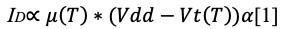
Where μ represents mobility and VTH represents threshold voltage. ID depends on Mobility (µ) and threshold voltage (VTH). The drain current is decided by the factor that influences it at a given temperature and voltage. Mobility decides the drain current at high supply voltages (VDD). At lower supply voltage (VDD) threshold voltage ( VT) influences and determines the drain current.
Mobility is the measurement of how fast the carriers (electrons or holes) can move through a semiconductor in the presence of an electrical field. Semiconductor mobility depends on the impurity concentrations, temperature, electrons, and hole concentrations. Mobility is the proportionality constant between an electric field and the drift velocity of the carriers in the conductive material. Depending on the quality of a semiconductor crystal, the number of impurities in the crystal, and the temperature.
Temperature inversion affects the Delay of cell
As mentioned, both the mobility and the threshold voltage decrease with increasing temperature. However, their effect on the drain current is reversed.
Lower mobility reduces the drain current.
Lower threshold voltage results in an increment in the (ID) drain current.
Decrement in threshold voltage (VTH) resulting in a reduction in cell delay.
Lowering mobility results in an increment in cell delay.
Threshold voltage (VTH) and mobility (µ) whichever will be dominant will determine the cell delay and whether the delay of the cell will rise or fall.
Effect of Temperature in lower technology node
In lower technology nodes, the supply voltage is less and the effect of temperature inversion can be seen. It can be seen in the above experiment, showing cell delay is decreasing with an increase in temperature. Therefore, the effect of VTH and mobility contribution is small on cell delay as Temperature increases.
The cell delay shows the opposite behavior to the temperature for lower node technologies as compared to higher technology nodes, decreasing for low in lower technologies as the temperature rises.
Mobility and threshold voltage are impacted by a temperature inversion, and these variables are reliant on the supply voltage. The threshold voltage effect predominates when the supply voltage is within the range that is comparable to VTH, whereas mobility predominates when the supply voltage is greater than VTH.
Temperature inversion is a phenomenon that has a significant impact on the performance of semiconductor devices, especially on lower technology nodes. In this article, we will discuss the basics of temperature inversion, its effects on device performance, and the strategies that can be used to mitigate its impact on lower technology nodes.
Effects of Temperature Inversion on Device Performance
Temperature inversion has several effects on device performance. One of the most significant effects is a reduction in carrier mobility. When minority carriers accumulate in the channel, they create a potential barrier that restricts the flow of majority carriers, reducing carrier mobility. This results in a decrease in device performance, including reduced saturation current, transconductance, and drain-induced barrier lowering.
Another effect of temperature inversion is an increase in gate leakage current. The high-density region of minority carriers in the channel region can create a conductive path between the gate and the source or drain regions, leading to an increase in gate leakage current. This can cause reliability issues and impact the overall performance of the device.
Strategies to Mitigate Temperature Inversion on Lower Technology Nodes
To mitigate the impact of temperature inversion on lower technology nodes, several strategies can be used. One common strategy is to use a low-k dielectric material to reduce the thermal conductivity of the device. This can help to minimize the temperature gradient across the device and reduce the likelihood of temperature inversion.
Another strategy is to optimize the device layout to reduce the thermal resistance of the device. This can be achieved by increasing the width of the device and reducing the length of the device, which can help to dissipate heat more effectively.
Conclusion
In summary, a temperature inversion is a significant challenge for semiconductor devices, particularly on lower technology nodes. Understanding the effects of temperature inversion on device performance and implementing strategies to mitigate its impact can help to improve the performance and reliability of semiconductor devices. By using low-k dielectric materials and optimizing the device layout, the negative impact of temperature inversion can be minimized, leading to better device performance and reliability.
Temperature Inversion#temprature #vlsi #inversion