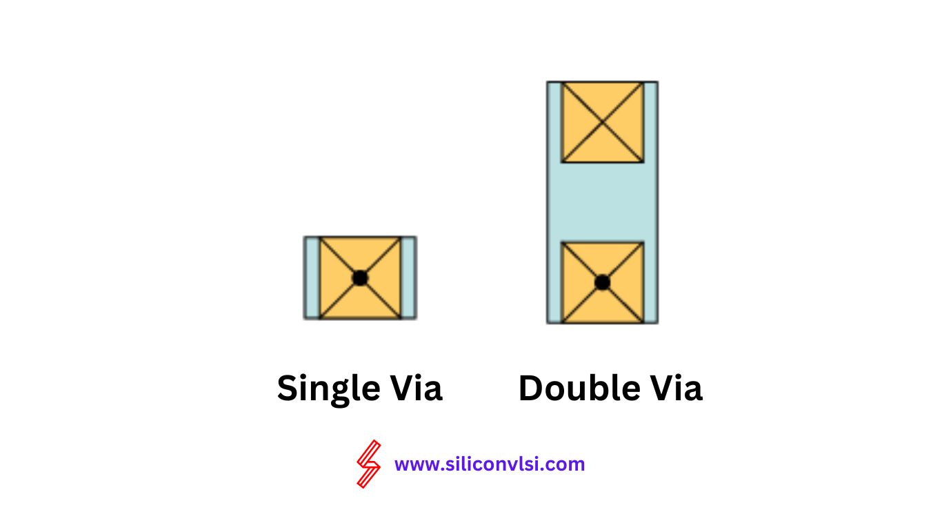
Via doubling is a practical strategy to help stem yield loss in semiconductor manufacturing. When a single via fails to make adequate electrical contact, it can cause an entire chip to fail, leading to serious consequences for your yield. That’s why we recommend using at least two vias for every connection between two metal layers, even if one via is technically sufficient to meet current carrying capacity requirements. By doing this, you ensure that the failure of one via won’t impact your overall yield. This increase in the number of vias is driven by shrinking structure sizes and the corresponding rise in complexity.
For instance, it is recommended to use a minimum of two vias for each connection between two metal layers, even if one via would meet the current carrying capacity requirements. Consequently, the failure of one of these vias would not impact the chip’s yield.
Three types of IC yield loss can be distinguished: parametric (timing-related problems), systematic (pattern dependencies in the layout), and random (often particle defects). A frequent design practice called doubling can increase yield in all three of these areas, despite the fact that various methods are being developed to address yield issues.
The cause of yield loss is determined by a statistical probability of occurrence, regardless of the mechanism (random, systematic, or parametric). Via failure rates typically fall below statistically significant thresholds, as indicated by faults per million or billion.
Maximizing Yield and Efficiency with Via Doubling in Chip Design
One effective technique that has gained traction is via doubling. By strategically placing a second via in the layout, designers can enhance chip performance without sacrificing valuable chip area. In this article, we will explore the benefits of via doubling and provide actionable tips to optimize its implementation.
Integrating Via Doubling into the Design Flow To ensure seamless integration of via doubling, it is essential to incorporate it into the normal physical verification flow. This allows for thorough design rule compliance (DRC) verification and facilitates determining the optimal method for doubling the via. By considering factors such as the direction of the second via, designers can streamline the design flow, especially since via doubling typically occurs towards the end of the design cycle when schedules are often compressed.
Leveraging Available White Space Doubling every via may lead to a significant increase in the design area, potentially rendering the design un manufacturable. However, by intelligently utilizing available white space, designers can minimize the impact on the design area. This practice involves optimizing the placement of second vias, and strategically locating them where feasible. By doing so, designers can achieve the desired performance improvements while keeping the design area in check.
Back-Annotation for Design Database Integration The addition of second vias can introduce parasitic effects, particularly in terms of capacitance. To evaluate the impact on timing and accommodate future engineering change orders, it is advisable to back-annotate the via-doubling modifications into the design database. This enables comprehensive parasitic extraction and simulation, ensuring any negative impact is identified and addressed promptly.
Statistical Reports for Design Validation To validate the design after placing the second vias, it is important to generate statistical reports through a comprehensive DRC run. This step provides assurance that the design remains acceptable for handoff to the foundry. By leveraging statistical analysis, designers can identify and rectify any potential issues before manufacturing, safeguarding the chip’s quality and performance.
Supporting Multiple Via Configurations In typical chip architectures, different metal layers are oriented in various directions. Relying on a single via configuration may not provide optimal coverage in such cases. Poorly located vias, particularly those placed near stress-induced voids, can lead to rapid failure. By introducing a second via, designers can disperse these localized effects, ensuring improved overall chip reliability.
Avoid These Pitfalls for Successful Via Doubling Implementation
While via doubling offers numerous benefits, it is essential to avoid certain pitfalls to ensure successful implementation. Let’s explore these potential challenges and how to address them effectively:
Making Via Doubling a Design Rule Automatically doubling every via is neither necessary nor advisable. Doing so would result in a substantial increase in the design area, which is an impractical trade-off for most designs. Given the low statistical nature of single-via failure, the excessive increase in design area outweighs the benefits of via doubling.
Integrating Via Doubling Beyond Place-and-Route Via-doubling coverage heavily relies on the tool’s ability to analyze the layout and determine optimal placement methods. Since layout inconsistencies are inherent, it is important to leverage a physical verification tool with a robust geometric-processing engine. This allows for examining various configurations and selecting the most efficient approach to minimize timing impact.
Avoiding Unnecessary Jogs Unnecessary jogs can introduce systematic defects arising from the interaction between layout patterns and process variations. These defects can create post-layout problems when lithographers apply resolution enhancement techniques for deep-submicron processes. Therefore, it is advisable to minimize unnecessary jogs, ensuring a smoother manufacturing process aligned.