Drain Induced Barrier Lowering (DIBL)
Drain Induced Barrier Lowering (DIBL) is a short channel effect in MOSFET prominent in ultra-scaled MOSFETs having a channel length less than 100 nm.
“If the drain voltage is increased, the potential barrier in the channel decreases, its called as DIBL”
The reduction of the potential barrier eventually allows electron flow between the source and the drain, even if the gate-to-source voltage is lower than the threshold voltage.
“The channel current that flows under these conditions (VGs<VT0) is called the sub-threshold current.”
Hence the sub-threshold current increases. Raising the drain potential increases the drain junction depletion region, reducing threshold voltage furthermore.

In an NMOS when a positive voltage is applied at the gate, the p-type channel starts to deplete. and If the gate voltage keeps on increasing, the channel undergoes inversion and starts conducting. This is the above threshold region. So, in conclusion, we can say that GATE voltage is solely responsible for depleting the charge in the channel and controls the threshold of MOSFET. Well, Yes this is true for Long Channel MOSFETs’.
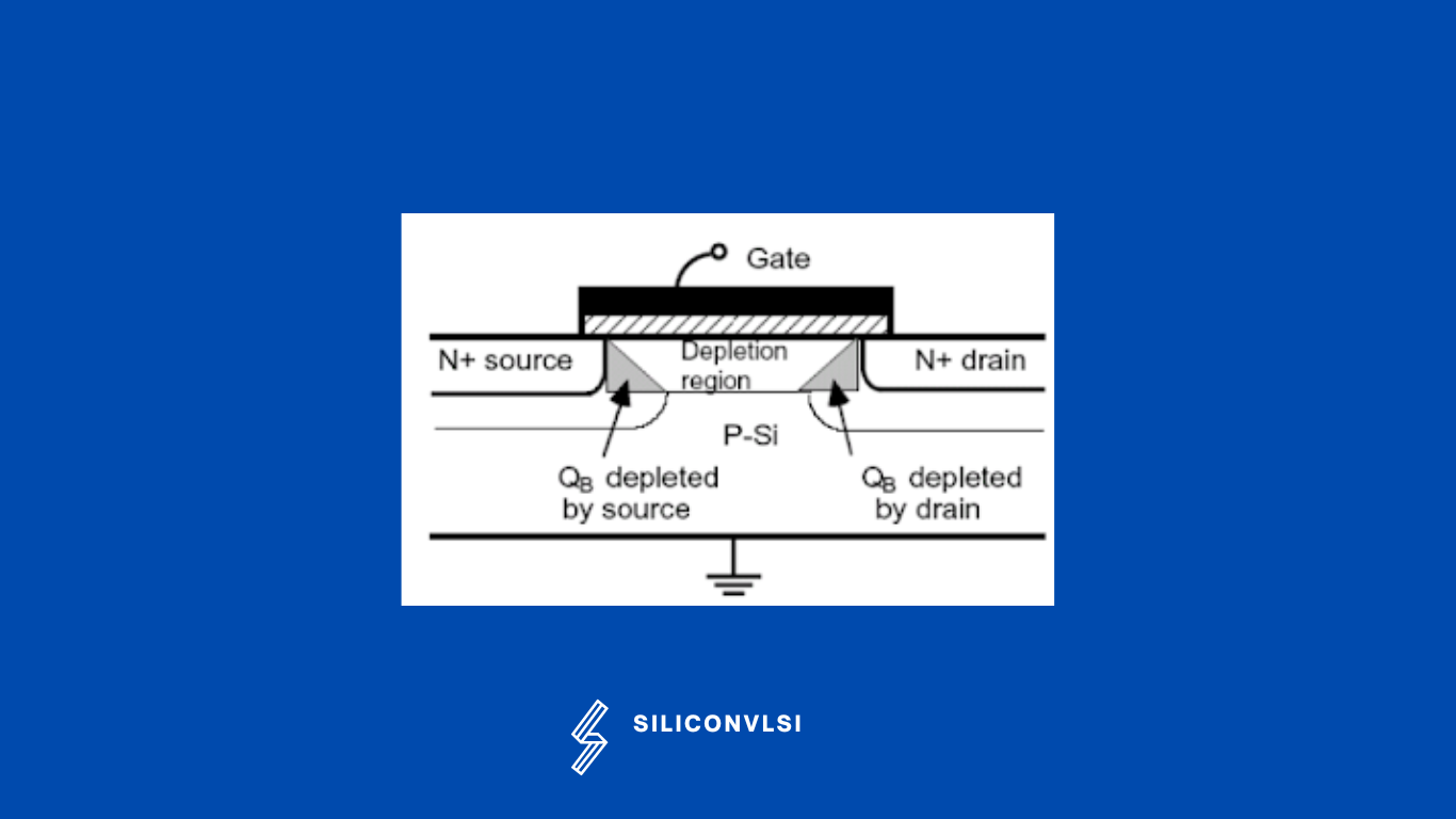
But in short Channel MOSFETs, there is a concept of ‘Charge Sharing’. Since the channel length is very small between the source and drain, any positive voltage applied at the Drain or Source will result in depleting a part of the channel region also. Hence the total effective charge that the MOSFET has to now deplete to turn the MOSFET ON is reduced. So, we can now achieve that by applying a smaller GATE voltage. Hence we say that the threshold voltage of MOSFET has decreased due to charge sharing.
Now, DIBL is basically a manifestation of this Charge Sharing. When the voltage on the Drain is increased the depleted region under the channel due to the Drain bias increases. Hence the threshold voltage decreases further. This is the DIBL effect which implies that the threshold voltage of a MOSFET decreases due to applied Drain bias.
Drain bias lowers the energy barrier between Source and Channel for electrons in a heavily doped Source. and Hence electrons from the source can easily go into the channel. In Long channel MOSFET, the only gate voltage is responsible for source-to-channel barrier lowering but in short channel MOSFET this is also induced by drain bias hence called ‘Drain Induced Barrier Lowering’
How is DIBL measured?
The net result is an increase in leakage current between the source and drain as the drain bias increases. DIBL is calculated by dividing the horizontal shift in the sub-threshold characteristics (measured in millivolts) by the change in the drain-to-source voltage (VD) on a log ID – VGS plot.