
What is an FPGA? Field Programmable Gate Array
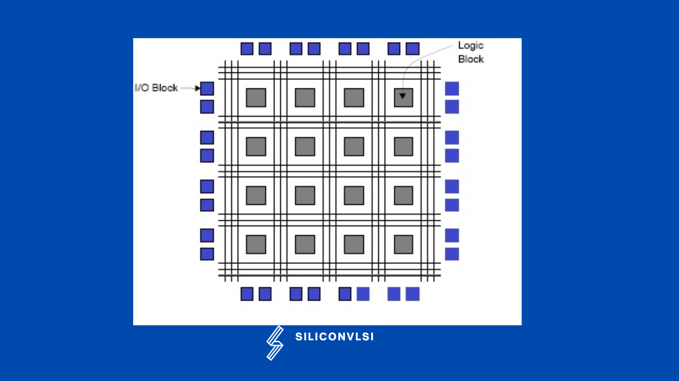
FPGA is called “Field Programmable Gate Array” and it contains ten thousand to more than a million logic gates with programmable interconnection. as the name suggests Programmable interconnections are available for users to perform given functions easily. A typical model FPGA chip is shown in the following given figure. There are I/O blocks, which are designed and numbered according to function. For each module of logic level composition, there are CLBs (Configurable Logic Blocks). The interconnection between CLB and I/O blocks is made with the help of horizontal routing channels, vertical routing channels, and PSM (Programmable Multiplexers).
The complexity of FPGA is decided by CLBs (Configurable Logic Blocks). The functionality of CLBs and PSM is designed by VHDL or any other HDL(Hardware Descriptive Language).
Types of FPGA
There are three types of FPGA.
Low-End FPGA
Low-end FPGA consumes less power than the other two and is less complex as the numbers of gates are less.
Mid-Range FPGA
It consumes more power than low-end FPGAs and has more gates, so it is more complex. It provides a balance between performance and cost.
High-End FPGA
It has a large gate density, so is more complex than mid-range. Their performance is better than low-end and mid-range FPGA.
FPGA Advantage :
- They are cost-efficient.
- FPGAs are reprogrammable.
- No physical manufacturing steps are involved in it
- FPGAs allow you to finish the development of your product in a very short time.
- FPGAs provide better performance than a general CPU and they are capable of handling parallel processing.
FPGA Disadvantages :
- High power consumption
- They are only used where the production volume is low.
- The programming of FPGA is not as simple as C programming.
FPGA Application:
- For ASIC prototyping,
- Image processing in SDRs,
- For diagnosis and therapy in the medical field.
- In wireless communication such as WiMAX, WCDMA, etc.
- In consumer electronics like flat panel displays, residential set-top boxes, etc.
What is the need for FPGA?
Developers select FPGA (Field-Programmable Gate Array) for various reasons. One key advantage is their versatility, allowing developers to test numerous variables after the board is built. When changes are needed, new configuration files can be transferred to the device, enabling new functionality without requiring hardware modifications. This flexibility enables OEMs (Original Equipment Manufacturers) to ship systems earlier in the design process.
FPGAs are commonly used in prototyping to incrementally refine designs before finalizing them at tape-out. They are also favored in commercial applications with dynamic requirements, such as telecoms and avionics, where parallel computing is essential.
Lower price points and other features make FPGAs suitable for many use cases. They are ideal for hardware prototyping, allowing verification of digital hardware designs without the upfront cost of ASIC (Application-Specific Integrated Circuit) manufacture. Additionally, FPGAs excel in hardware acceleration, where custom hardware implementation speeds up designs.