
Why do we use p substrate in CMOS?
Starting with a p-type substrate allows one to build n-channel transistors without additional doping. That is the main advantage of the P substrate.
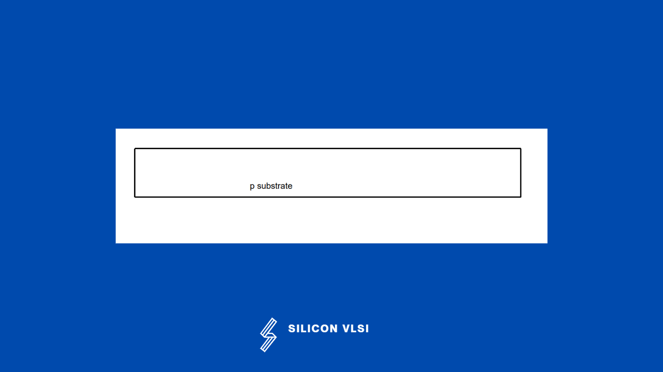
Reason for used P-substrate in CMOS
NMOS is faster than PMOS, because the carriers in NMOS, which are electrons, travel twice as fast as holes, which are the carriers in PMOS. Now P substrate has the majority carrier is holes, now if we are using an n-substrate, we need to form a p-well inside to form NMOS, now as we have hole mobility, less than electrons, now we need to form a p-well by counter doping, so with that again we are decreasing hole mobility, so it may degrade the performance of NMOS, so we are using p substrate in CMOS.
The second reason is that if we create a P-well above the N-type substrate, to get maximum electron mobility in NMOS we need a very high resistive (high doping) P-well, which is a costly process. So, the fastest NMOS was obtained with a high resistive P substrate, not a lower P-well in an N-type substrate.
The third reason is in a p-well technology, such a choice would degrade the gain due to the body effect of pMOS transistors (coming as a second cause for gain degradation after the “low mobility of holes” cause).
The fourth reason is, The p-type doping of an original silicon wafer is more uniform than any doping that can be obtained by introducing a p-well into a silicon wafer. The only methods to create a p-well are by diffusion or ion implantation and both have inherent non-uniformity with depth into the substrate.
The fifth reason is p-type substrate allows one to build n-channel transistors without additional doping. This is a substantial advantage because, the lower the doping, the higher the mobility of electrons and the higher the gain, and the higher the switching speed of transistors.
The sixth reason is the p substrate is less suspect to noise as compared to the n substrate. #
The seventh reason is if We use n substrate then the whole plate needs to be tied with power(VDD), which may create leakage.
What is a p-type semiconductor?
An inherent semiconductor doped with boron (B) or indium is known as a p-type semiconductor (In). Boron from Group III has three valence electrons, while silicon from Group IV has four.