
Layout & Stick Diagram Design Rules in VLSI
The layout is a physical representation of circuit design, or The Layout is a drawing of the masks which will be used in the manufacturing process.In VLSI, a stick diagram is a kind of diagram used for transistor cell layout. In stick diagrams, the devices and conductors are represented by “sticks” or lines. The direction and metalization of the input, output, ground, and power supply must be specified to design the circuit architecture.
Layout Design Rule Understanding
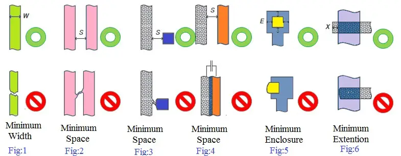
Minimum width
The minimum size is necessary for each physical layer to prevent a structure from falling into the Fabrication process. If we are not following minimum width then electrically dis joint will create after some time and it will divide into pieces shown in figure 1. According to DRM(Design rule Manual), there is some minimum width defined. It varies based on technology.
Minimum spacing
Short circuits between adjacent layers are avoided by putting minimum spacing limits between layout structures on a single conducting layer. please have a look at figure 1 2 3. If we did not put a certain space then it will create a short in-between. Again this minimum spacing value depends on technology.
Minimum enclosure
Minimum enclosure requirements are uniform in all directions and apply to layout structures on different layers. They ensure that the layers involved in contact or via link are properly despite minor mask misalignment and etching process tolerances in the case of contact or via.
Minimum extension
For Some Layers, we should give some extension from the layer edge to avoid silicon failure. For example, Why we are giving poly extension from the diffusion edge? The answer is: During the Fabrication process, for diffusion fabrication(by ion implantation) step, Poly(gate) acts as a mask for diffusion. so if we do not extend the poly over diffusion, there might be chances of mask misalignment during the fabrication, and it will create a short between source and drain, so we must give poly extension from the diffusion. Here important point is that the polysilicon gate acts as a mask during the implantation of the source and drain.
Layout Basic Layer Information
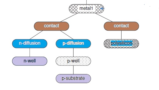
(1) Substrates or Wells: For NMOS devices, these wells or substrates are p-type, while for PMOS devices, the well is n-type.
(2) Diffusion areas: Transistors will be produced in these regions, which are also known as active layers. These are denoted by the letters n+ for NMOS transistors and p+ for PMOS transistors.
(3) Polysilicon layers: These are employed to make the transistors’ gate electrodes.
(4) Metals: This is used for connection from base layers to top-level
Important Points for Layout Design Engineer
Use more number of vias, and if there is not much area then put single rectangular via instead of single square via.
- Put the device far from the Well edge to avoid Well Proximity Effect
- Put the device in the same proximity
- Share the device with having a common node
- Use shielding for critical nets
Stick Diagram
The usage of stick diagrams, often known as symbolic layouts, can greatly simplify the initial step of layout creation. The essential elements (active areas, polysilicon lines, metal lines) are represented by constant-width rectangles or simple sticks, while the precise layout design criteria are simply ignored.
The stick diagram’s objective is to provide the designer with a thorough knowledge of the topological limitations and to allow them to quickly test numerous options for the best arrangement without having to build a complete mask diagram.
A stick diagram in VLSI (Very Large Scale Integration) design is important because it helps designers document the layout and layers of electronic chips. Stick diagrams use colors or simple patterns to show different parts of the chip.