What is Critical area analysis(CCA)
Critical area analysis (CAA) can be used during design and verification to improve the yield of the design and improve the Design for Manufacturing (DFM).
Design for Manufacturing (DFM) and Design for Reliability (DFR) are important steps to confirm and improve a product’s ability to be produced and to be reliable. Critical Area Analysis can be used to carry out this evaluation (CAA). In this study, the Defect Per Million (DPM) reliability data which is determined from the number of customer field return units is associated with the CAA results.
In order to determine whether the failure locations are within the critical region, we used a differentiator technique that involved analyzing the defects and hot spot location of the failed unit and mapping the location to the CAA heat map. A high DPM rate set of products were used for the analysis.
Critical Area Analysis (CAA), a concept integral to yield modeling since its inception in the 1980s, is fundamentally tied to defect size. It represents the region where the center of a defect of a certain size falls, potentially causing functional failure in integrated circuits (ICs). Over the years, CAA has evolved beyond its initial purpose and is now utilized for various applications.
Moreover, with the advent of FinFET nodes, new challenges have emerged, including transistor-related defectivity and interlayer interactions. Pegasus CAA aims to tackle these challenges head-on by incorporating FinFET failure models, enhancing efficiency in critical area extraction, and developing innovative methodologies and applications to address the intricacies of modern semiconductor manufacturing processes.
![]()
Performing CAA is important for products used in the automobile industry that have high dependability requirements. In addition to the physical verification required by the Design Rule Check, automobile designers must also confirm their Design Rule Check (DRC). The method employed in this study was to map the Failure Analysis Request (FAR) hot spot position from the customer’s field return to the CAA heat map,
which we called FAR doting. In CAA, the assessment is carried out using a unique reliability-oriented DRC. The goal of this work is to promote robust DFM and DFR using CAA to discover design layout flaws and obtain feedback on how well the design is performing in terms of robustness.
Critical area analysis Methodology
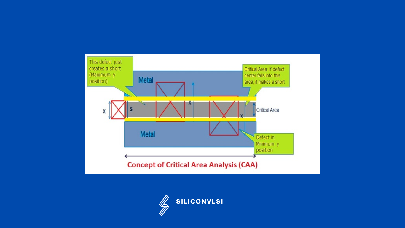
In order to identify locations that might be more vulnerable than average to defects caused by random particles, CAA examines the physical layout of an IC. The fundamental concept is that conductive or non-conductive particles fall on the circuit at random locations, and depending on their conductivity, size, and placement, they may produce an electrical OPEN or SHORT and ultimately a circuit failure.

In the above figure, If X is less than S, then no short will form, but if X is greater than S then there might be chances to short. The region where the fault center must be situated in order to establish a SHORT or OPEN is noted on the standard CA.
The reliability of the system will be in danger if the problem is not in the CA region but is almost there or close to its edge. In this case, there will be no SHORT or OPEN isolation gap, only a small one. The reliability of CA’s perimeter is a measure of its sensitivity to these near SHORT or near OPEN events(In the above figure, yellow region).
Critical Area Analysis on Single Via
The CAA analysis can also produce the opportunity to identify defective single via where there is potentially enough space for double via insertion in order to make the interconnect more robust. OPEN connections or connections with high resistance are typically the results of poor via creation caused by via stress points, random particles at the position of the via, or both.
Placing two or redundant via at each transition is a straightforward approach. However, the double via may have an effect on design size that must be considered, such as whether the single via is in the logic region. Thus it is also expected that the Analog circuits might allow double or multiple via to ensure high reliability and better DFM, and this is not expected to take up more space as most analog circuit has large dimensions.
References
[terminal]K. K. S. Joseph, T. B. Heng and M. Hanno, "Critical Area Analysis of IC layout for automotive application," 2016 IEEE International Conference on Semiconductor Electronics (ICSE), 2016, pp. 296-299, doi: 10.1109/SMELEC.2016.7573650.[/terminal]