
What is FinFET?
Why do we need FinFET Technology?
As the sizes of the devices shrunk, in lower technology nodes, for example, 22nm, with the scaling in channel length, area, power, and operating voltage, the short channel effects started becoming more dominant, and also its reducing the performance of the device. To overcome this issue, a new FET design named “FinFET” is developed.
When Transistor is in OFF condition and since the gate controls the channel from both sides, the leakage is reduced better than in a planar CMOS transistor. This is one of the main advantages of this FinFET technology.
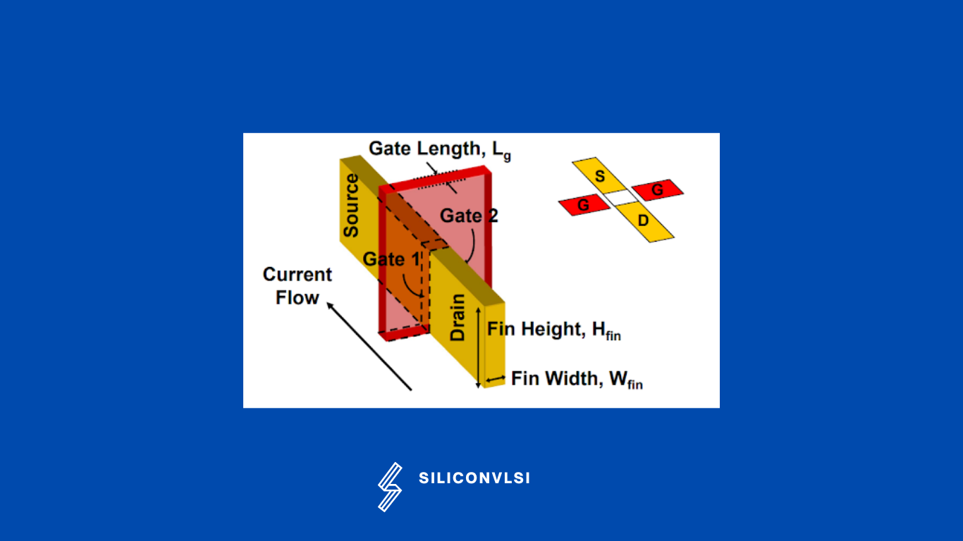
Effective Channel Width = (2 * Height of Fin) + Thickness of the fin
W= (2*H) + w
Effective Channel Length = Length of the gate = L
Advantages of FinFETs over CMOS
- Very good gate control of the channel even at low voltages.
- FinFETs have lower DIBL so they reduced sub-threshold leakage.
- Short-channel effects are very few.
- Channel doping is less so that less dopant-induced variations and better performance.
- It is able to work at a lower operating voltage
- Better performance for a given power budget.
- For memory designs, FinFETs have lower retention voltage for SRAMs compared to planar.
Disadvantages of FinFET over CMOS
- FinFETs are complex devices to model.
- Width quantization
- Accurate FinFET parasitic extraction is more complicated than a planner.
- FinFETs are 3D structures that need a high aspect ratio
- The body biasing techniques is not applicable to FinFET.
FinFETs: Advantages, Processing Complexity, and Key Steps
FinFETs offer several advantages over advanced planar transistors, including lower leakage, higher speeds, lower VDD (drain-source voltage), lower power consumption, and improved scaling. However, these advantages come with certain drawbacks, primarily related to the complexity and cost of their fabrication.
Processing Complexity
- Three-Dimensional Channels: FinFETs have a three-dimensional channel structure, which adds complexity to the manufacturing process. Unlike planar transistors, which have a flat channel, FinFETs require precise control over the fin’s topography.
- Gate Stack Formation: Forming a well-behaved gate stack on the fin is challenging due to the fin’s unique shape. Achieving uniformity in gate stack deposition and patterning is critical.
- Low-Resistance Source/Drains: Creating low-contact resistance source/drains, crucial for transistor performance, adds significant complexity to FinFET processing.
Fabrication Steps
Silicon Fin Etch: In a Silicon-On-Insulator (SOI) FinFET process, the silicon fin etch is not timed, as the underlying Buried Oxide (BOX) serves as an etch stop layer. The goal here is to form uniform width and height fins, with heights typically being twice or more the width, often around 10 nm in advanced processes.
Shallow Trench Isolation (STI): Similar to conventional CMOS, adjacent devices must be isolated, and local overlying interconnects must be isolated from the substrate. This is achieved through STI, involving the following steps:
Deposition of CVD oxide to overfill trenches formed by the fins.
Planarization of the overfill oxide using Chemical Mechanical Polishing (CMP).
Timed etch to recess the trench oxide and expose the sidewalls of the fins.
Gate Stack Formation: The gate stack is crucial for transistor operation and includes these steps:
Formation of a high-quality oxide on the exposed fin surfaces to serve as the gate dielectric.
Deposition of gate electrode material, often polysilicon.
Patterning of the gate through a controlled etch process, with the hardmask protecting the fins during this step.
Implants: Masked implants are performed to create punchthrough suppression regions and heavily doped source and drain regions, similar in principle to conventional CMOS.
Silicidation: Following source and drain formation, silicidation processes are carried out to improve contact resistance.
Back-End-of-Line (BEOL): BEOL processes involve forming interconnects to connect and wire the transistors into functional circuits.
In summary, while FinFETs offer significant performance advantages, their complex three-dimensional structure and the intricacies of processing steps, especially gate stack formation and source/drain creation, make their manufacturing more challenging and costly compared to planar devices.