Device isolation Techniques in VLSI
For the isolation of neighboring MOS transistors there exist two techniques, namely Local Oxidation of Silicon(LOCOS) and Shallow Trench Isolation(STI).
Local Oxidation of Silicon(LOCOS)
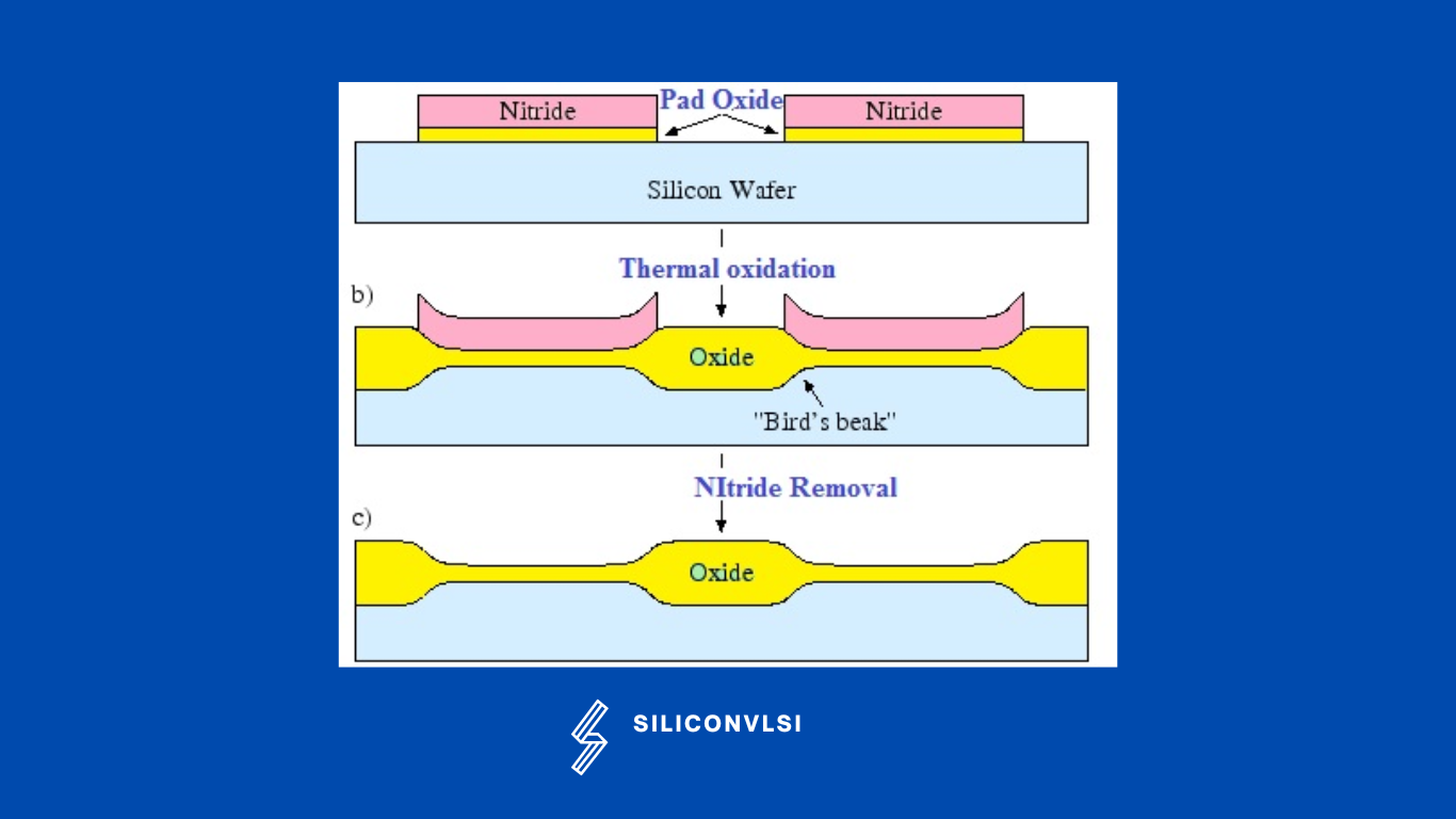
Local Oxidation of Silicon (LOCOS) is the traditional isolation technique. The first step is a very thin silicon oxide layer is grown on the wafer, called as pad oxide. Then a layer of silicon nitride is deposited which is used as an oxide barrier. This pattern transfer is performed by photolithography. After lithography, the pattern is etched into the nitride. The result is the nitride mask as shown in the following figure(1), which defines the active areas for the oxidation process.
The second step is the main part of the LOCOS process, which is the growth of the thermal oxide.
The last step is the removal of the nitride layer. The main drawback of this technique is the bird’s beak effect and the surface area which is lost to this encroachment. The advantages of LOCOS fabrication are the simple process flow and the high oxide quality because the whole LOCOS structure is thermally grown.

What is the primary purpose of the LOCOS (Local Oxidation of Silicon) process in semiconductor manufacturing?
The primary purpose of the LOCOS process is to create a diffusion barrier of silicon nitride that blocks the thermal oxidation of specific regions on the surface of a semiconductor wafer. It is commonly used in CMOS technologies with minimum linewidths of half a micron or larger.
How does silicon nitride serve as a barrier in the LOCOS process, and what properties make it suitable for this purpose?
Silicon nitride serves as a barrier because both oxygen and water diffuse slowly through it. This property allows silicon nitride to be deposited and patterned to define active and field oxide areas effectively.
What is one of the primary limitations associated with the LOCOS process, and how does it affect circuit packing density?
One of the primary limitations of the LOCOS process is bird’s beak encroachment. Bird’s beak encroachment occurs when the lateral diffusion of the oxidant forms an oxide feature that extends into the active area, reducing the achievable circuit packing density.
Shallow Trench Isolation (STI)
Shallow Trench Isolation (STI) is the preferred isolation technique for deep sub-micron technology because it completely avoids the bird’s beak shape characteristic.STI is more suitable for the increased density in a small area because it allows forming smaller isolation regions. The STI process starts in the same way as the LOCOS process. The first difference compared to LOCOS is that a shallow trench is etched into the silicon substrate, as shown in Figure 1.
After under etching of the oxide pad, also with the help of thermal oxide in the trench is grown, the so-called liner oxide is shown in the following figure 2,3.
![]()
The thermal oxidation process is stopped after the formation of a thin oxide layer, and the rest of the trench is filled with a deposited oxide in the following Figure 4.
Next, the excessive (deposited) oxide is removed with chemical mechanical planarization. and the last the nitride mask is also removed. The price for saving space with STI is the larger number of different process steps.
![]()
So in conclusion we can say that STI is best for the device isolation process as compared to the LOCOS process.
Why is STI preferred over LOCOS?
We concluded that Shallow Trench Isolation (STI), in which the original field oxide abruptly projects above the substrate surface, offers an advantage over LOCOS not only in terms of isolation space reduction but also in reducing alignment tolerance.
What is the primary purpose of the Shallow Trench Isolation (STI) process in semiconductor manufacturing?
The primary purpose of the STI process is to achieve isolation between different regions on a semiconductor wafer, particularly in sub-half-micron CMOS technologies. It involves etching shallow trenches into the wafer’s surface and filling them with a dielectric material, serving as the field oxide (FOX).
How does the STI process minimize active-area encroachment and what advantage does it offer in terms of thermal budget?
The STI process minimizes active-area encroachment, ensuring that isolation structures do not intrude significantly into the active regions. Additionally, it has a relatively low thermal budget, which means it involves processes with lower temperatures, minimizing the impact on device performance.
Can you describe the typical sequence of steps involved in the STI module of semiconductor manufacturing?
The STI module typically begins with thermal oxidation of the wafer surface, creating a pad oxide layer. Silicon nitride is then deposited onto the oxidized wafer, serving as an implant mask and CMP stop-layer. Photolithography is used to define active areas, and the photoresist pattern is transferred into the underlying nitride and oxide layers using RIE (Reactive Ion Etching). Subsequently, shallow silicon trenches are etched, and the photoresist and etch by-products are removed to complete the STI structure.
Why is the presence of photoresist during the silicon trench etching step important, and what benefit does it provide?
The presence of a photoresist during silicon trench etching is important because it helps tailor the sidewall profile of the trenches, allowing for a specific slope. These sloped sidewalls aid in reducing leakage current from parasitic corner transistors, albeit at the cost of reduced packing density