

Triple-Well Processes
Triple-Well Processes are used to isolate the most sensitive circuit in Analog Layout Design. A triple-well structure contains at least one p-well in a p-type substrate, and a number of deep n-wells, and inside the deep n-well, a p-well is formed as shown in Following Figure 1.
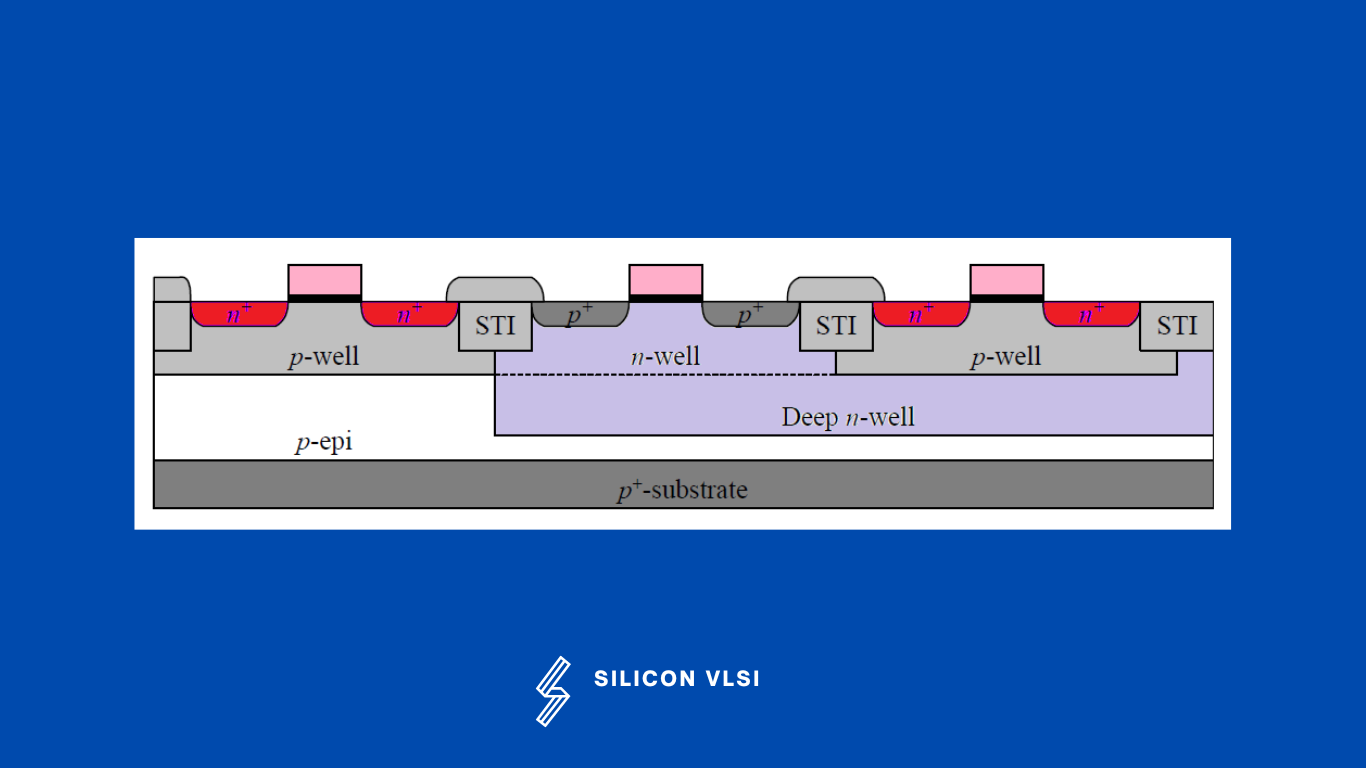
Why we need Triple-well structure in CMOS.
As we know that we are using Guarding and Epitaxial Layer in Analog Devices for device isolation purposes, but it helps to provide isolation from the surface only, Because of coupling capacitance, and capacitance from the substrate or ground side, we need Tripe Well structure in CMOS.
Triple-Well Fabrication Processes.
The triple-well structure can be formed using either diffusion, called the diffused triple well, or high-energy ion implantation called the retrograde triple well. Due to many advantages over the diffused triple well, the retrograde triple-well structure has dominated and been widely used in modern CMOS devices, including memory and embedded memory.
The first Fabrication step is, too deep the n-well is fabricated by ion implantation, with high energy, Second step is to fabricate N-well and P-well(inside the deep n-well). The process for fabricating the triple-well structure begins to form deep n-wells with high-energy ion implantation in the p-type substrate at a depth.
The n-well mask is subsequently used to form n-wells at a depth of about 1 mm where p-type MOS transistors are to be fabricated. The threshold voltage adjustment of pMOS transistors is also done in this step. Then, the p-well mask is employed to form p-wells where n-type MOS transistors are to be fabricated. These p-wells are at about the same depth as n-wells. The threshold voltage adjustment of nMOS transistors is also done in this step. Finally, a high-temperature drive-in process is applied to form p-wells and n-wells.
Advantages of triple-well process
It helps to avoid coupling capacitance from the substrate or ground. #
It also avoids band-to-band leakage current at the source junction during the erase operation.
It provides an electrically isolated P-well in order to reduce the electronic noise and cross-talk from the substrate.
Epitaxial Layer
An epitaxial layer wafer provides a low-resistance substrate that helps significantly to reduce the possibility of latch-up.
7 Key Advantages of Triple-Well CMOS
1. Better Substrate Noise Isolation
One of the most important benefits is improved isolation from substrate noise.
A deep n-well can help prevent noise generated by nearby digital circuits from coupling directly into a sensitive p-well.
2. Reduced Substrate Coupling
Unwanted signals can propagate through the silicon substrate through resistive and capacitive coupling paths.
Triple-well structures provide additional junction isolation and can reduce these coupling paths.
However, triple-well technology does not eliminate substrate coupling completely.
3. Improved Analog Circuit Performance
Sensitive analog circuits can benefit from a cleaner local substrate environment.
This can be important for circuits where small disturbances can affect:
- Offset
- Noise
- Linearity
- Reference accuracy
- Timing
- Phase noise
4. Better Isolation Between Circuit Blocks
Triple-well structures are useful when noisy and sensitive blocks must coexist on the same chip.
For example, a mixed-signal IC may contain:
Digital block → noisy switching environment
and
Analog block → sensitive circuit
The deep n-well can help isolate the analog NMOS devices from substrate noise generated by the digital section.
5. Improved Control of the NMOS Body
In a triple-well structure, the isolated p-well can have its own body connection.
This provides greater flexibility in controlling the NMOS body potential compared with an NMOS whose body is tied directly to the common substrate.
It can also be useful in circuits that require body-biasing techniques.
6. Reduced Risk of Substrate-Related Interference
By adding well isolation and appropriate contacts/guard structures, designers can reduce the influence of unwanted substrate signals.
Triple-well technology is therefore particularly valuable in high-performance analog and mixed-signal layouts.
7. Useful for Mixed-Signal and RF Designs
Triple-well structures are commonly valuable where digital switching activity exists close to sensitive analog or RF circuitry.
Typical applications include:
- ADCs
- DACs
- PLLs
- VCOs
- RF circuits
- Sensor interfaces
- Power-management circuits
- Precision analog blocks
Triple-Well and Guard Rings
A triple-well structure should not be considered a replacement for good layout practices.
Guard rings, proper substrate contacts, well contacts, shielding, and careful floorplanning can work together with triple-well isolation.
For example:
Sensitive NMOS → isolated p-well → deep n-well → substrate
Additional well and substrate contacts provide controlled bias connections.
The effectiveness of the isolation depends strongly on the process, layout geometry, contact placement, and circuit environment.
Triple-Well and Epitaxial Layers
An epitaxial layer is a separately grown silicon layer used as part of certain semiconductor wafer structures.
An appropriately engineered epitaxial/substrate structure can influence:
- Substrate resistance
- Latch-up behavior
- Parasitic bipolar action
- Substrate noise propagation
However, an epitaxial layer and a triple-well structure solve related but different isolation problems.
Triple-well: primarily provides well/junction isolation and control of the local body region.
Epitaxial structure: affects the electrical properties of the underlying silicon and can influence substrate coupling and latch-up behavior.
Does Triple-Well Completely Eliminate Substrate Noise?
No.
This is an important point.
Triple-well technology can significantly improve isolation, but it does not create perfect electrical isolation.
Noise can still couple through:
- Junction capacitance
- Interconnect capacitance
- Supply connections
- Common substrate paths
- Package coupling
- Electromagnetic coupling
Therefore, triple-well should normally be combined with proper analog layout techniques.
Triple-Well vs Guard Ring
| Feature | Guard Ring | Triple-Well |
|---|---|---|
| Substrate isolation | Moderate | Better local isolation |
| Layout area | Requires additional area | Can require significant area |
| Body control | Limited by surrounding structure | Better control of isolated p-well |
| Substrate noise reduction | Yes | Yes, generally stronger |
| Process requirement | Widely available | Requires triple-well/deep-n-well option |
| Typical use | General isolation | Sensitive analog/mixed-signal blocks |
The two techniques can also be used together.
Triple-Well in Analog Layout
When using a triple-well device in analog layout, designers should pay attention to:
Well Contacts
Provide appropriate contacts to keep the deep n-well and isolated p-well at their intended potentials.
Guard Structures
Guard rings can provide additional protection against substrate noise and unwanted injected currents.
Spacing
Follow the foundry’s spacing and enclosure rules for:
- Deep n-well
- P-well
- N-well
- Active regions
- Contacts
- Guard rings
Routing
Avoid unnecessarily routing noisy high-slew-rate signals close to sensitive analog nodes.
Floorplanning
Place sensitive circuits inside appropriate isolation structures and keep noisy digital blocks away whenever possible.
Triple-Well Process: Important Design Considerations
The exact implementation of a triple-well structure is process-dependent.
There is no universal rule for:
- Well depth
- Implant energy
- Doping concentration
- Mask sequence
- Well spacing
- Deep n-well dimensions
- Required guard-ring structure
These values are determined by the foundry’s process technology and PDK.
For physical design, the PDK documentation and design rules should always be treated as the final authority.
Common Misconceptions About Triple-Well
Does triple-well mean three separate transistor wells?
Not necessarily.
The term generally refers to the combination of substrate, deep-well, and nested well structures. The exact interpretation depends on the process technology.
Is deep n-well only used for isolation?
No.
Besides isolation, a deep n-well can provide an isolated body region and can be useful for body-biasing and other circuit techniques.
Does triple-well eliminate latch-up?
It can improve isolation and may help with latch-up robustness, but it should not be described as a complete latch-up solution.
Proper well ties, guard rings, spacing, and process-specific rules remain important.
Is triple-well available in every CMOS process?
No.
Triple-well or deep-n-well capability is a technology option and must be supported by the particular foundry process and PDK.
Frequently Asked Questions
What is a triple-well process in CMOS?
A triple-well process is a CMOS technology that uses a nested well structure, commonly a deep n-well containing an isolated p-well, to provide improved electrical isolation and body control.
Why is triple-well used in analog layout?
It helps reduce substrate coupling and noise from nearby circuits, making it useful for sensitive analog and mixed-signal blocks.
What is the purpose of a deep n-well?
A deep n-well can isolate a p-well from the surrounding substrate and provide better control of the electrical environment around NMOS devices.
What is retrograde triple-well?
A retrograde triple-well uses implantation conditions designed to create a well with a non-uniform dopant profile, typically with a relatively higher concentration deeper in the silicon.
Does triple-well reduce crosstalk?
It can reduce substrate-mediated coupling, which may reduce one source of unwanted interference. It does not eliminate capacitive or electromagnetic crosstalk through other coupling paths.
Is a guard ring still required with triple-well?
Not necessarily in every design, but guard rings and well/substrate contacts are often used together with triple-well structures for additional isolation and robust biasing. The exact requirement depends on the process and circuit.
Conclusion
The triple-well process is an important CMOS technology option for improving isolation in sensitive analog, mixed-signal, and RF circuits.
The key idea is to use a deep n-well with an isolated p-well so that the body region of an NMOS can be separated more effectively from the common substrate.
Its major benefits include improved substrate-noise isolation, better body control, and reduced substrate coupling.
However, triple-well is only one part of a robust layout strategy. Guard rings, well contacts, shielding, floorplanning, spacing, and correct biasing are still important for achieving reliable circuit performance.