Close Menu
  • Analog Design
    • Latest Analog Layout Interview Questions (2025)
  • Digital Design
    • Digital Electronics Interview Question(2025)
    • Top VLSI Interview Questions
  • Physical Design
    • Physical Design Interview Questions for VLSI Engineers
  • Verilog
    • Verilog Interview Questions(2024)
  • Forum
Facebook Instagram YouTube LinkedIn WhatsApp
SiliconvlsiSiliconvlsi
Forum Questions Register in Forum Login in Forum
Facebook Instagram YouTube LinkedIn WhatsApp
  • Analog Design
    • Latest Analog Layout Interview Questions (2025)
  • Digital Design
    • Digital Electronics Interview Question(2025)
    • Top VLSI Interview Questions
  • Physical Design
    • Physical Design Interview Questions for VLSI Engineers
  • Verilog
    • Verilog Interview Questions(2024)
  • Forum
SiliconvlsiSiliconvlsi
Home»VLSI Design»What Is Double Patterning in VLSI?
VLSI Design

What Is Double Patterning in VLSI?

siliconvlsiBy siliconvlsiJanuary 10, 2022Updated:July 16, 2024No Comments2 Mins Read
Facebook Pinterest LinkedIn Email WhatsApp
Share
Facebook Twitter LinkedIn Pinterest Email

What Is Double Patterning in VLSI?

“To achieve higher density and better resolution in layout, we used double patterning”

Double patterning is a widely used technique in advanced semiconductor manufacturing processes, especially at smaller process nodes. This technique involves using lithography methods to define the features of integrated circuits more precisely. By employing double patterning, designers can fabricate chips at sub-nanometer process nodes, ensuring high performance and functionality. The double patterning process typically involves litho-etch-litho-etch (LELE) pitch-splitting steps within the fabrication facility. Another approach known as self-aligned double patterning (SADP) utilizes spacer methods as part of the double patterning process, enabling even greater precision in feature definition.

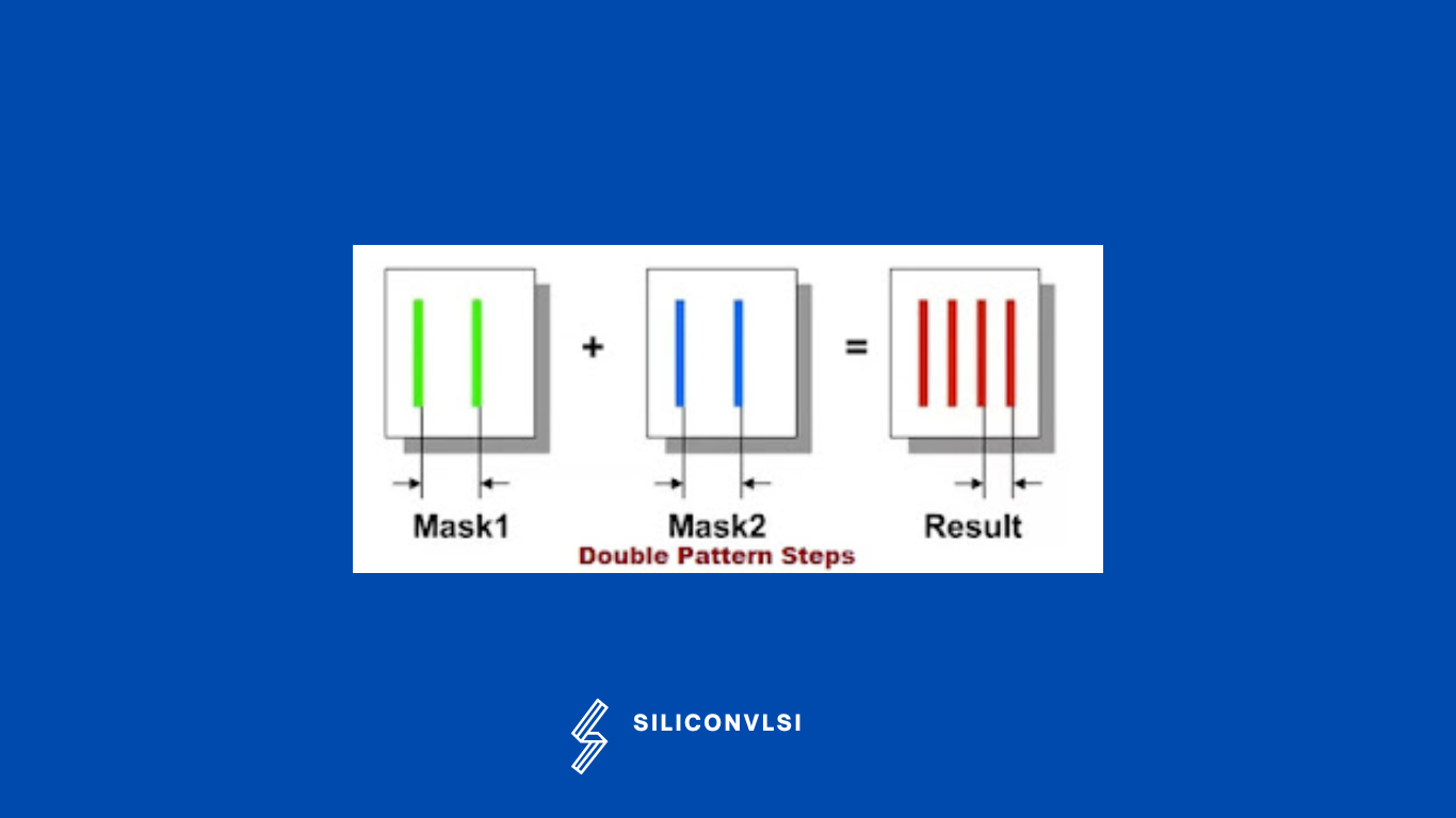
The fabrication of MOSFETs is done using light of wavelength 193nm in a process called Optical lithography. Now as we move towards lower technology nodes i.e. channel length below 30nm, the process can lose its accuracy. The quality is lost due to the diffraction of light around the corners and edges of the mask since the features are too small compared to the wavelength of light. This results in uneven edges, shorts, or the complete absence of the metal to be etched. This is where double patterning comes into the picture.

Double patterning in VLSI

In this method, dense patterns of metals in a single mask are split into 2 different masks that can be interleaved to get the original pattern as desired. and the masks are identified by assigning colors to the metals (red and green as shown in the following figure). Since the masks are fabricated separately this can be corrected. This way we can get better resolution and higher layout density.

Double patterning in FINFET
Double pattern techniques are very useful in lower nodes like FinFET. 


Share. Facebook Twitter Pinterest LinkedIn Tumblr Email

Related Posts

How Shielding Avoids Crosstalk Problem? What Exactly Happens There?

September 22, 2024

Navigating the Challenges of Gate Dielectric Scaling in MOS Transistors

August 1, 2024

Challenges in Modern SoC Design Verification

April 20, 2024
Leave A Reply Cancel Reply

Facebook X (Twitter) Instagram Pinterest Vimeo YouTube
  • About Us
  • Contact Us
  • Privacy Policy
© 2025 Siliconvlsi.

Type above and press Enter to search. Press Esc to cancel.