
Decoupling Capacitor Insertion: Minimizing IR-Drop Violations
Decap cells are basically charge-storing devices made of substrate capacitors and used to support the instant current requirements in the power delivery network. Decoupling capacitors called DECAP cells, on the other hand, are used to isolate two stages of a circuit so that these two stages don’t have any DC effect on each other.
Decap cells are mostly used in power distribution networks. After doing Layout, LVS, and DRC clean, we need to fill the remaining empty part with decap cells, it will help in two ways, it will help to improve IR drop, and also it will help to maintain density-related DRC error.
What is Voltage Drop and Ground Bounce?
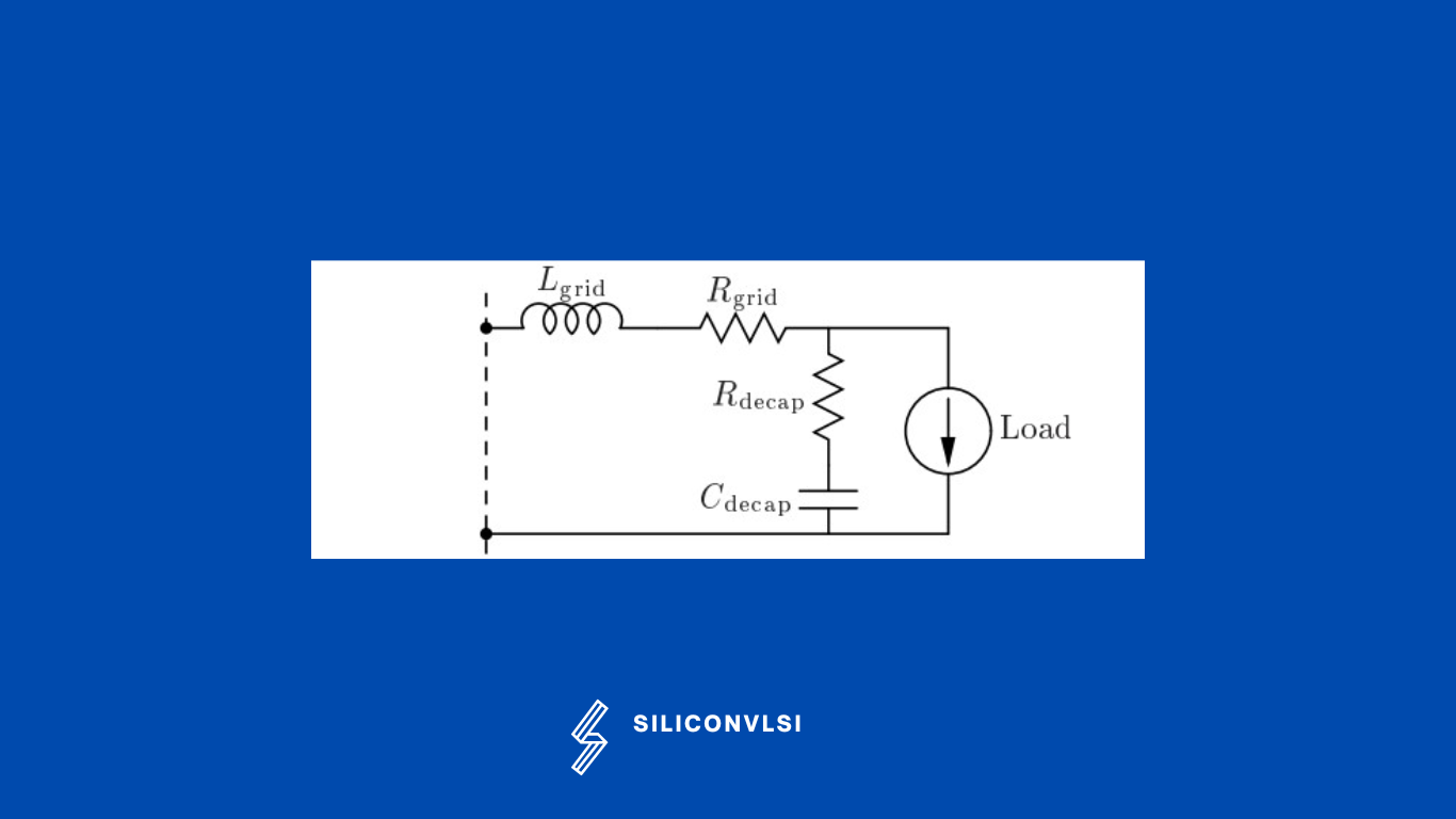
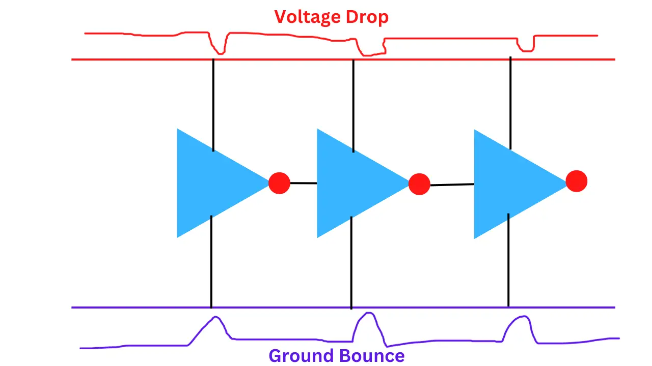
In a large circuit, the large current requirement will drop the VDD or may increase the ground voltage which is called voltage droop or ground bounce as shown in the following Figure, this phenomenon will come in any VLSI circuit.
Ground bounce is usually seen on high-density VLSI Layout, where insufficient precautions or bad power mesh have been taken to supply a logic gate with a sufficiently low resistance connection to the ground. Voltage droop or ground bounce may result in a change in the delay of the circuit, and this delay may further affect the timing of the design
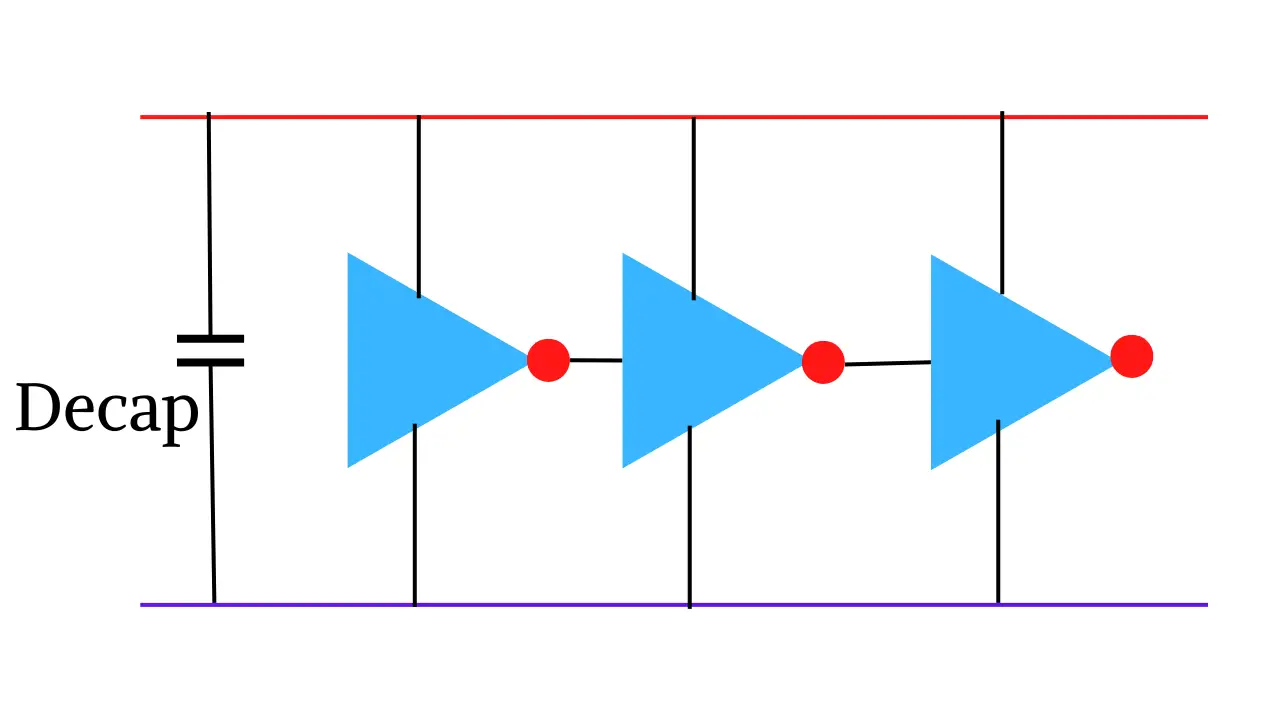
To avoid the Voltage Drop and Ground Bounce, we are using DECAP cells. Decap cells work as charge reservoirs and support the power delivery network and making it robust and will help in to provide the protection of the circuit. Sometimes in the ESD circuit also,decap (GGNMOS)cells are used.
The Role of Decap Cells in Semiconductor Design
- In Analog and Digital Layout.
- Decap cells are used charge storing device
- Help to improve Voltage drops and Ground Bounce.
- Use for Maintain Density related DRC error in Layout design.
Placement of Decap cells.
Decap cells are often installed during the pre-placement stage, which comes after the power planning and before the installation of regular cells. In this step, these cells are distributed consistently throughout the design. If necessary, decap cells can also be added at the post-route step.
Drawback of Decap Cells
Decap cells are leaky
Increases the leakage power of design.
The Role of Bypass Capacitors in Circuit Design
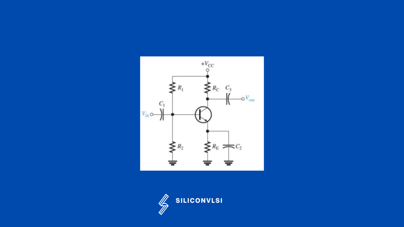
The coupling capacitor is used to maintain the DC biasing condition of the circuit but cannot pass DC through it. So that the DC voltage at different terminals remains the same. Whereas, the by-pass capacitor is used to pass the AC which passes through the resistor so that the effective gain will be higher for the same circuit. In the following Figure, C1, and C3 are coupling capacitors and C2 is a by-pass capacitor.
The bypass capacitor helps us meet this requirement by constraining unwanted communications like noise. Any glitch or noise appearing on the power line is immediately bypassed into the chassis ground and thus prevented from entering into the system, hence the name bypass capacitor. So in short bypass capacitors help us avoid noise reduction.
What is the difference between decoupling and bypass capacitors?
The decoupling capacitor primarily serves to store energy and then release it back into the power rail, ensuring a steady flow of current. On the other hand, the bypass capacitor is responsible for providing an AC signal return path, allowing for the efficient switching between the power and ground rails. In essence, while both capacitors contribute to stabilizing the power supply, the decoupling capacitor focuses on maintaining a continuous power flow, whereas the bypass capacitor aids in facilitating the return path for AC signals.