
Deep Sub-Micron
DSM means Deep Sub-Micron. Nowadays, in VLSI, technology is reducing day by day to improve the PPA(Power performance and area). The feature size of the individual transistor is shrinking from the deep sub-micrometer (DSM).
As a result, the operating frequency and processing power per chip expand steadily, causing an increase in power dissipation. These pressures of circuit integration evolution create a requirement for low-power VLSI chips.
Low power requirements result from the market’s rising demand for portable consumer electronics powered by batteries and consumers’ desire for smaller, lighter, and more durable electronic items. Low-power CMOS VLSIs are increasingly used in portable multimedia terminals with speech and handwriting recognition capabilities, notebook computers, and digital personal communication services.
What is DSM in VLSI design?
As VLSI technology shrinks to deep sub-micron (DSM) geometries (below 0.18µm), the parasitic effects caused by interconnects are increasingly limiting circuit performance.
Deep Sub-Micron Effect
There are some main effects, which we will discuss in this article,
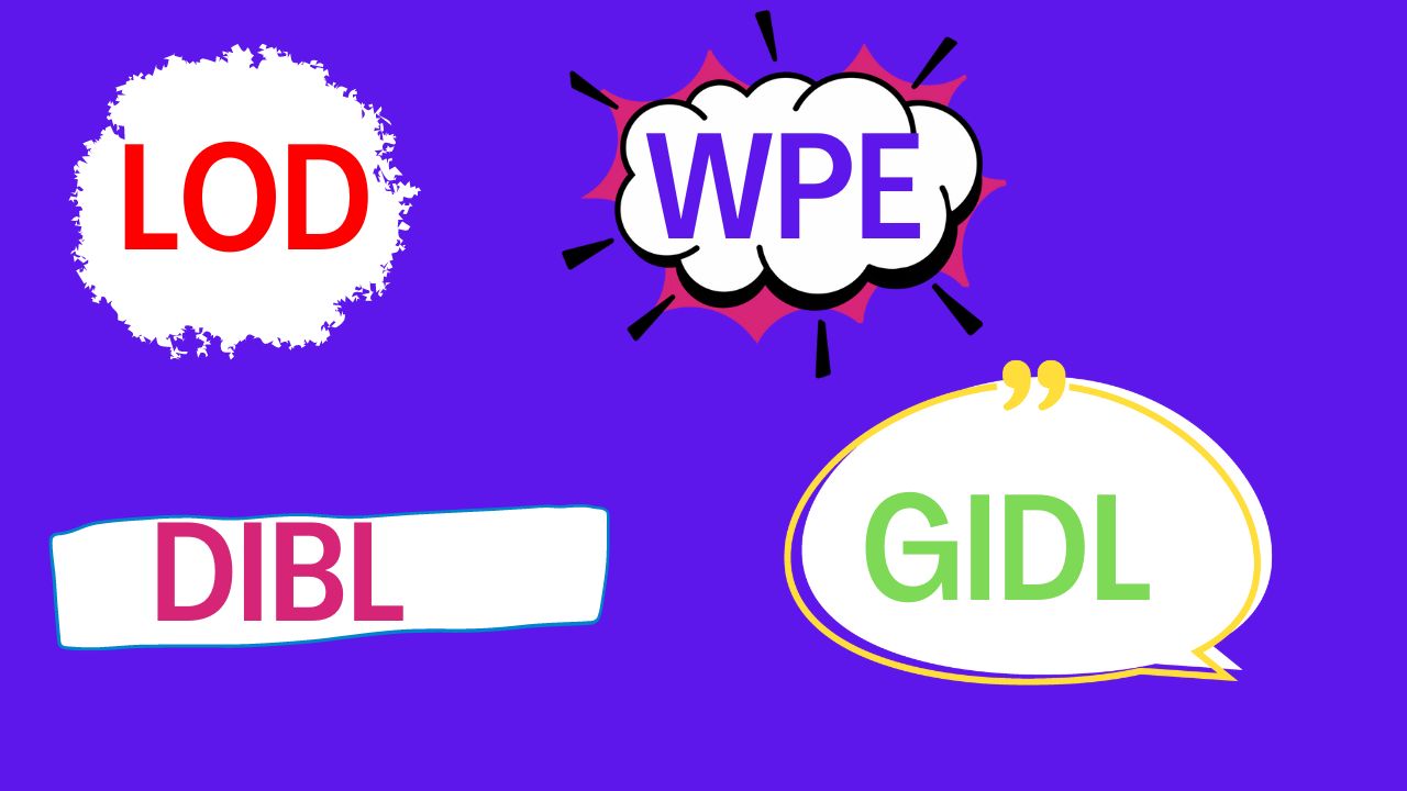
- LOD(Length Of Diffusion effect)
- WPE(Well proximity effect)
- Hot carrier effects
- Velocity saturation
- Impact ionization
- DIBL
- GIDL
- Punch through
- Tunneling effects
LOD(Length Of Diffusion effect)
During the STI(Shallow Stretch Isolation) process, Some mechanical stress will induce diffusion, and due to that Diffusion will get shrink, this is called a Length Of Diffusion effect. LOD is also called a layout-dependent effect in CMOS.
By etching the wafer and filling it with silicon oxide to act as isolation between active areas, the shallow trench is created during the transistor isolation process. This creates compressive stress that applies to the vicinity, or diffusion zones, using mechanical force. This stress is also known as the Length of Diffusion (LOD) effect and is frequently referred to as STI stress.
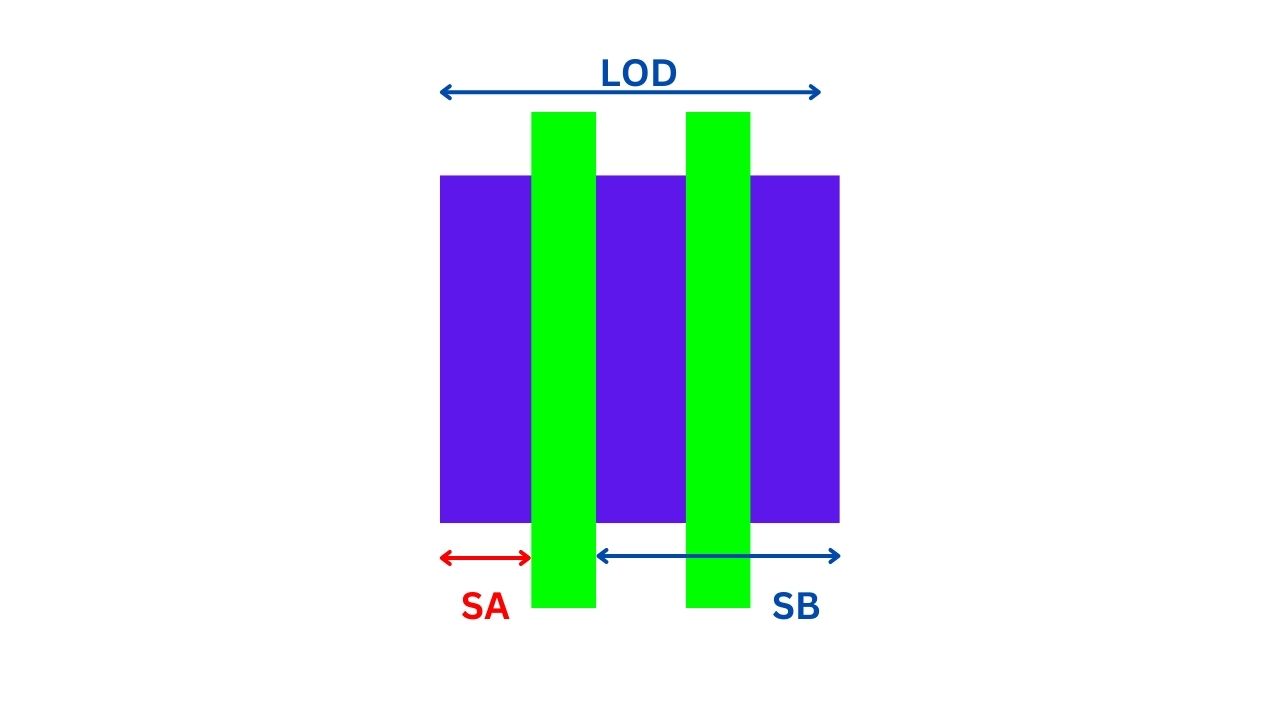
Shallow Trench Isolation Fact
- Wider STI the higher the stress.
- In Nature, STI becomes compressive as the wafer cools down.
- The width of STI (Active to Active Spacing) has a strong impact on determining stress.
Stress/strain definitions
Because of stress effect.
- NMOS-favor of tensile stress.
- PMOS-favor of compressive stress.
-
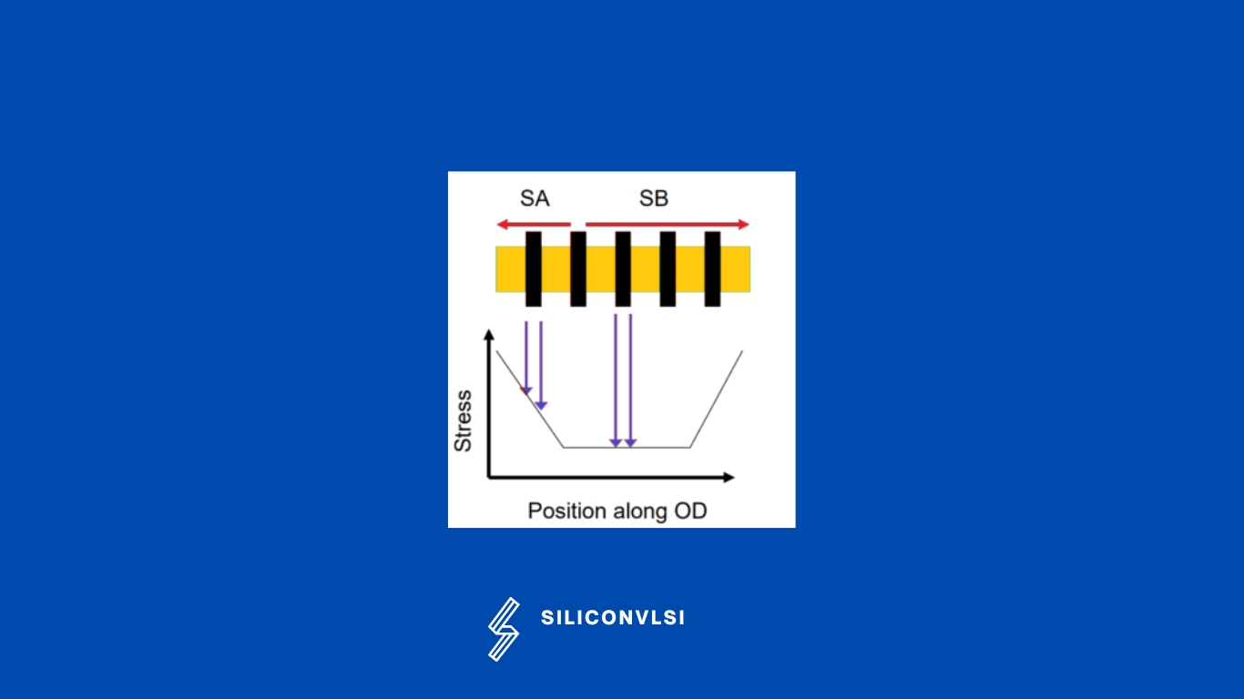
Stress vs position
The impact of shallow trench isolation (STI) proximity on device performance was one of the first stress-related effects to be researched and studied. Compressive stress is created on the area of the active device through STI creation. An idealized stress profile for two distinct OD lengths is shown above along with channel position (LOD).
The distance between the device channel and both STI edges affects the stress that the device detects. The stress is cumulative when both edges are close. Due to the compressive stress that STI causes, being close to the STI edge reduces NMOS performance while improving PMOS performance.
How to avoid the LOD(Length of Diffusion) Effect
- Use Dummy device
- Draw square Layout
- Put the device far from the WELL edge
- Avoid Multiple figures of devices
Velocity saturation
The velocity saturation will happen due to surface scattering. In velocity saturation, Id will be constant. This behavior causes the current IDS to become saturated as well, however, it usually affects short-channel MOSFETs (the channel length being smaller than in the previous device). Since mobility is regarded as a constant property, the velocity of carriers should change linearly with the applied electric field.
However, in a short channel, the carriers have too many collisions, which causes their velocity to saturate after a certain electric field. Since the current is the rate at which electrons flow, it also reaches a saturation point when the velocity increases.
Impact ionization
In Impact ionization, the process in the material by which one energetic charge carrier can lose energy by the creation of other charge carriers. Three particles are produced by the impact-ionization process. High-energy carriers that pass through high-field regions experience scattering interactions with bound electrons in the valence band.
This electron receives the extra energy and is then hoisted into the conduction band, forming a new electron-hole pair. Additionally, the energy of this secondary electron-hole pair may be quite significant. The avalanche effect is activated in this situation, greatly increasing the carrier density.
Punch-through effect in MOSFET
Reverse bias is provided to the drain in the punch-through mechanism, resulting in a longer depletion area. As a result, the two depletion regions of the drain and source meet, creating “one” depletion region that allows leakage current to flow and ultimately causes MOSFET breakage.
Tunneling effects
In the tunneling effect, the particles penetrate through the potential barrier even if the particle’s total energy is less than the barrier height.