
Different regions of operation in MOS Transistors
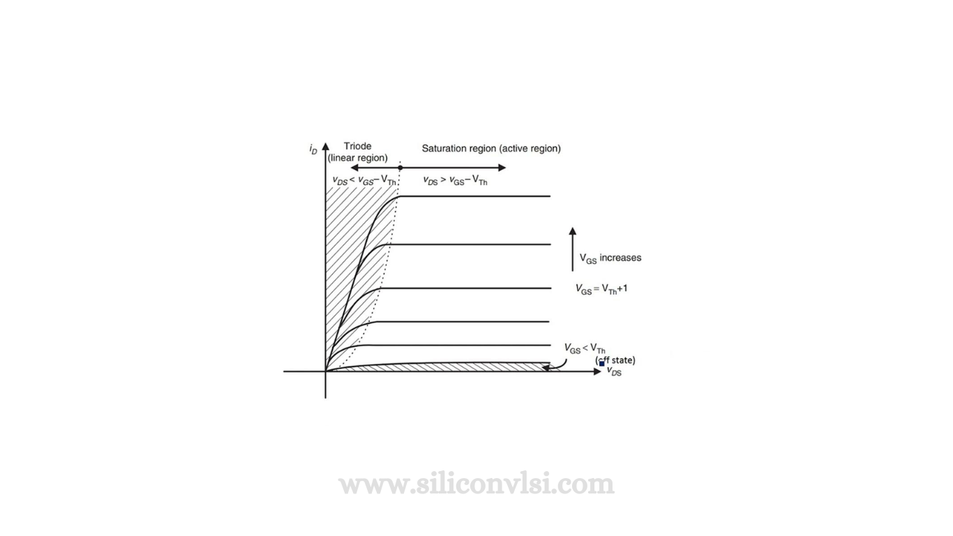
MOS transistors exhibit distinct regions of operation, notably the linear (or triode) region and the saturation region. In the linear region, characterized by low drain-to-source voltages, the MOS channel behaves resistively, and the drain current increases linearly with voltage. This is similar to the saturation region in bipolar transistors. As the drain-to-source voltage surpasses the difference between the gate-to-source voltage and the threshold voltage, the transistor enters the saturation region. Here, the drain current levels off to an approximately constant value.
The saturation region is associated with pinch-off, a phenomenon where a depletion region of uniform thickness surrounds the channel. As the drain voltage increases, the depletion region thickens at the drain end, intruding into and narrowing the channel. When the channel depletes entirely, it is said to have pinched off. Carriers move down the channel due to a weak electric field until reaching the pinched-off region, where a strong electric field propels them across the depletion region. This causes the drain current to reach a limit and cease to increase.
Interestingly, in the saturation region, the drain current curves tilt slightly upward due to channel length modulation, equivalent to the Early effect in bipolar transistors. Increased drain voltage widens the pinched-off region and shortens the channel, intensifying the electric field and causing carriers to move more rapidly, resulting in a slight increase in drain current.
The MOS transistor’s behavior is also affected by the back gate effect, where the back gate-to-source voltage modulates the depletion region beneath the channel. This modulation, known as the body effect, influences the apparent threshold voltage of the transistor. If the back gate is biased independently, the threshold voltage varies.
Furthermore, MOS transistors, considered majority carrier devices, exhibit subthreshold conduction just below the threshold voltage. The gradual formation of a channel allows minority carriers to move by diffusion, producing currents smaller than in the presence of a channel but still significant. This subthreshold conduction becomes problematic in low-V devices.
MOS transistors can experience breakdown through avalanche or punch-through. The operating voltage is often limited below the onset of these breakdown mechanisms by hot carrier injection, a long-term degradation mechanism. Hot carriers accelerated in the pinched-off portion of the drain, can become trapped in the gate oxide, leading to a shift in the threshold voltage over time. Techniques are employed to mitigate hot carrier injection in MOS transistors.
What is the linear region of operation in a MOS transistor?
The linear region of a MOS transistor corresponds to low drain-to-source voltages, where the drain current increases linearly with voltage. This region is also known as the triode region and roughly corresponds to the saturation region of a bipolar transistor.
Why do MOS transistors saturate, and what is the role of pinch-off in this phenomenon?
MOS transistors saturate due to pinch-off, where a depletion region begins to thicken at the drain end as the drain voltage increases. Eventually, the channel depletes, and carriers move across the pinched-off region, limiting the drain current.
Explain the upward tilt in drain current curves in the saturation region of MOS transistors and the role of channel length modulation.
The upward tilt is caused by channel length modulation, equivalent to the Early effect in bipolar transistors. Increases in drain voltage cause the pinched-off region to widen, shortening the channel and intensifying the electric field, leading to a slight increase in drain current.
What is the back gate effect in MOS transistors, and how does it affect the apparent threshold voltage?
The back gate effect, or body effect, occurs when the back gate is biased independently of the source. If the back gate-to-source voltage increases, the depletion region beneath the channel widens, affecting the apparent threshold voltage. NMOS and PMOS transistors exhibit different behaviors based on the back gate bias.
Describe subthreshold conduction in MOS transistors and its significance in low-V devices
Subthreshold conduction occurs just below the threshold voltage as minority carriers move from source to drain by diffusion. While this conduction is smaller than channel-formed currents, it can cause leakage issues in low-V devices. However, its usage is limited as junction leakages become overwhelming at temperatures exceeding 100°C.