Close Menu
  • Analog Design
    • Latest Analog Layout Interview Questions (2025)
  • Digital Design
    • Digital Electronics Interview Question(2025)
    • Top VLSI Interview Questions
  • Physical Design
    • Physical Design Interview Questions for VLSI Engineers
  • Verilog
    • Verilog Interview Questions(2024)
  • Forum
Facebook Instagram YouTube LinkedIn WhatsApp
SiliconvlsiSiliconvlsi
Forum Questions Register in Forum Login in Forum
Facebook Instagram YouTube LinkedIn WhatsApp
  • Analog Design
    • Latest Analog Layout Interview Questions (2025)
  • Digital Design
    • Digital Electronics Interview Question(2025)
    • Top VLSI Interview Questions
  • Physical Design
    • Physical Design Interview Questions for VLSI Engineers
  • Verilog
    • Verilog Interview Questions(2024)
  • Forum
SiliconvlsiSiliconvlsi
Home»VLSI Design»Fixing Double-patterning Errors in FinFET(2024)
VLSI Design

Fixing Double-patterning Errors in FinFET(2024)

siliconvlsiBy siliconvlsiFebruary 10, 2023Updated:December 29, 2024No Comments3 Mins Read
Facebook Pinterest LinkedIn Email WhatsApp
Share
Facebook Twitter LinkedIn Pinterest Email

Fixing Double-patterning Errors in FinFET(2024)

ODD Cycle Error in VLSI Layout

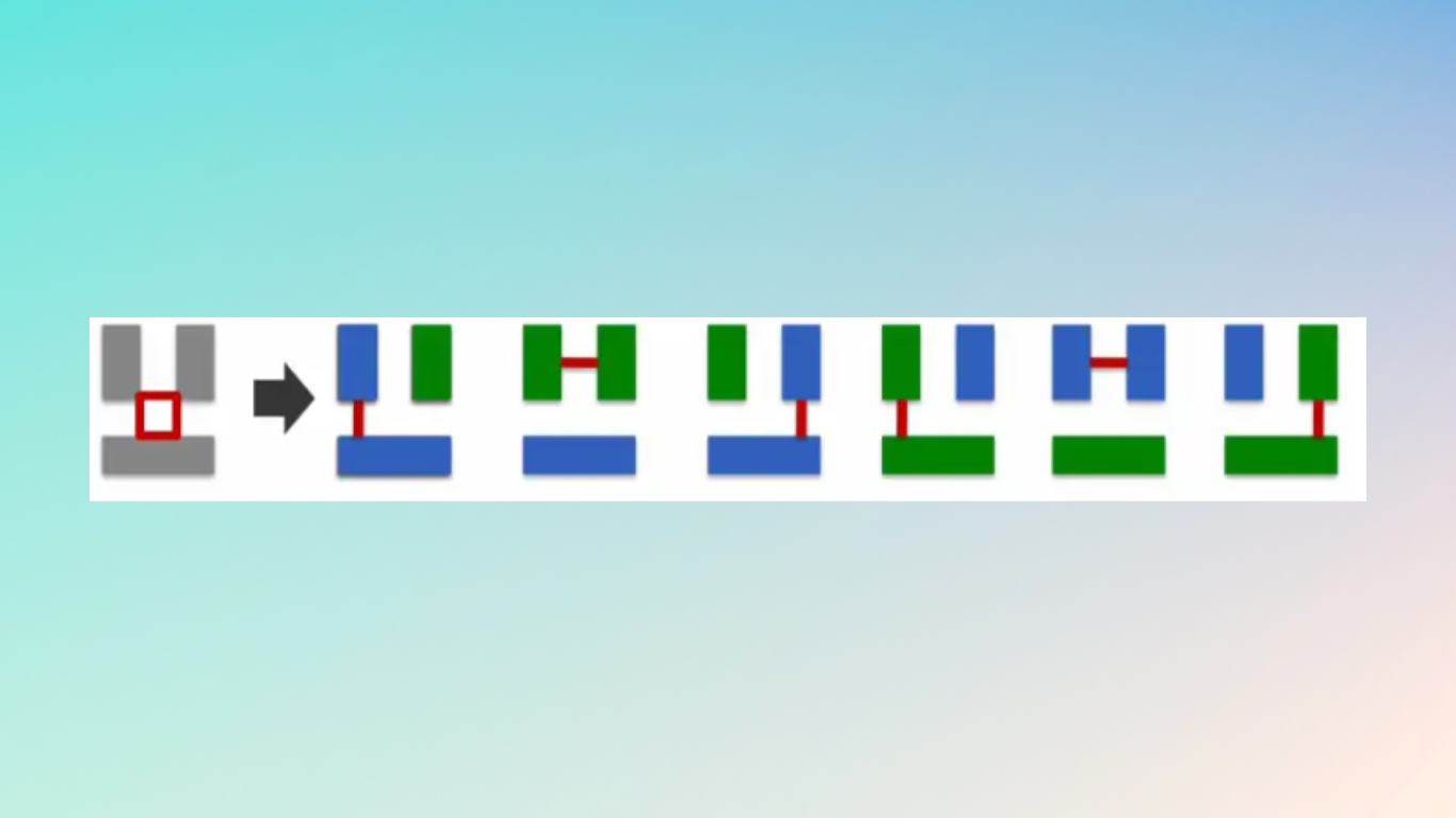
The so-called odd-cycle path is the most typical double patterning error. This occurs when an odd number of polygons are placed in a loop with a minimum spacing between them (technically, a spacing close enough to call for the polygons to be on separate colored masks).

G0(GNOT) Error in VLSI

In the most basic scenario, three polygons must each have a different color from the other two, which is obviously difficult given that there are only two colors available. It is important to stress that there are multiple violations, not simply one involving spacing or one involving color. The polygons are impossible to color correctly. The violation is indicated by a square (or more complex polygon for more complex violations) that identifies the cycle’s polygons rather than using a fictitious coloring to call attention to one of the violations as “the” error (as in the above picture).

How to Fix Double-patterning Errors

The violation can be fixed by either increasing spacing so as to break the cycle, or by removing a polygon completely, either breaking the cycle or making the cycle even (which is not a problem since it can be colored).

Fixing Double-patterning Errors1

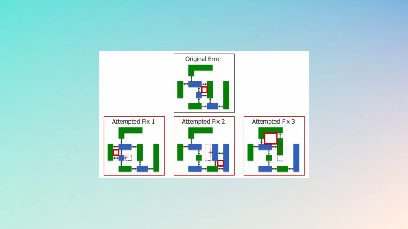
Of course, a real layout could contain both anchor path violations and odd path violations in the same area of the design. David suggests focusing on the unusual cycle path violations first because they frequently correct some of the anchor path violations anyhow. Consider your anchor path violations after that.

Why do we go for FinFET?

FinFETs have a structure that results in lower leakage power and higher device densities. They provide a high drive current and work at a lower voltage as well. By combining these factors, substantially more performance may be fit into a smaller space, lowering the cost per unit of performance.

How does FinFET reduce leakage?

FinFET transistors, in contrast, have a thin vertical fin with the gate completely encircling three of its sides. This leads to significantly improved channel control and, thus, less leakage.

What is better than FinFET?

In comparison to fin technology, nanosheet-based GAAFETs offer a higher driving current for the given footprint. In comparison to finFETs, the stacking of nanosheets enhances the effective channel width and the drive current capability of the device.

Where is FinFET technology used?

A transistor is a FinFET. It is both an amplifier and a switch because it is a transistor. Home computers, laptops, tablets, cellphones, wearable technology, high-end networks, automobiles, and more are just a few examples of its applications. Field-effect transistors with fins are referred to as FinFETs.
How to Resolve Double-Patterning Errors in FinFET Devices (2025)
Share. Facebook Twitter Pinterest LinkedIn Tumblr Email

Related Posts

How Shielding Avoids Crosstalk Problem? What Exactly Happens There?

September 22, 2024

Navigating the Challenges of Gate Dielectric Scaling in MOS Transistors

August 1, 2024

Challenges in Modern SoC Design Verification

April 20, 2024
Leave A Reply Cancel Reply

Facebook X (Twitter) Instagram Pinterest Vimeo YouTube
  • About Us
  • Contact Us
  • Privacy Policy
© 2025 Siliconvlsi.

Type above and press Enter to search. Press Esc to cancel.