
PN Junction Diode and Diode Characteristics
A p-n junction diode is a two-terminal semiconductor device, which allows the electric current in only one direction while blocking the electric current in the opposite direction. If the diode is forward-biased, it allows the electric current to flow. On the other hand, if the diode is reverse-biased, it blocks the electric current flow. A P-N junction semiconductor diode is also called a p-n junction semiconductor device.
There are main two types of basic semiconductors. One is n-type & other is p-type. In n-type semiconductors, free electrons are the majority charge carriers whereas, in p-type semiconductors, holes are the majority charge carriers. When the n-type semiconductor is joined with the p-type semiconductor, a p-n junction is formed. The p-n junction, which is formed when the p-type and n-type semiconductors are joined, is called as p-n junction diode.
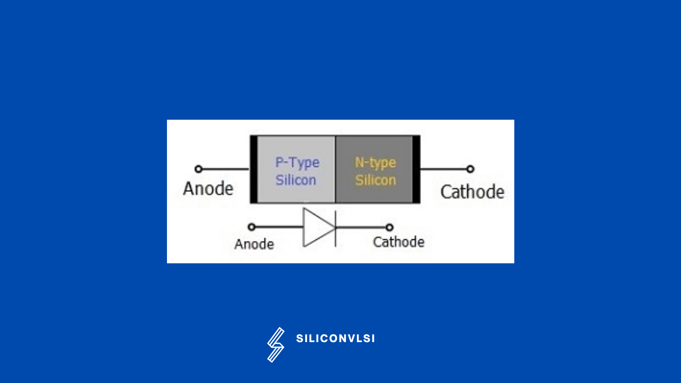
The p-n junction diode is made from the semiconductor materials such as silicon, germanium, and gallium arsenide. For designing the diodes, silicon is preferred over germanium because silicon semiconductors work at a higher temperature when compared with the p-n junction diodes made from germanium semiconductors. The nature of free electrons and holes is, that the free electrons moving from the negative terminal (cathode) to the positive terminal (anode) actually carry the electric current.
The free electrons are attracted towards the anode terminal or positive terminal whereas the holes are attracted towards the cathode terminal or negative terminal.
Forward Bias PN Junction Diode
In the forward-biased p-n junction diode, the p-type is connected to the positive terminal, and the n-type is connected to the negative terminal, the anode terminal is a positive terminal whereas the cathode terminal is the negative terminal.
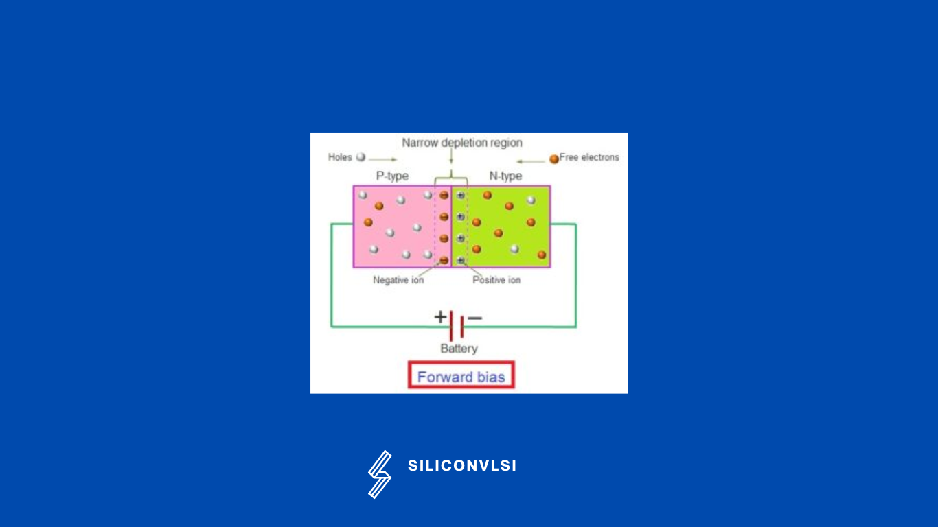
If the voltage applied on the p-n junction diode is further increased, then an even more number of free electrons and holes are generated in the p-n junction diode. This large number of free electrons and holes further reduces the depletion region. Hence, the electric current in the p-n junction diode increases. Thus, the depletion region of a p-n junction diode decreases with an increase in voltage. In other words, the electric current in the p-n junction diode increases with the increase in voltage. This is called as the forward bias of the PN junction diode.
Reverse Bias PN Junction Diode
If the diode is reversely biased, The p-type is connected to the negative terminal, and the n-type is connected to the positive terminal, the anode terminal becomes a negative terminal whereas the cathode terminal becomes a positive terminal.
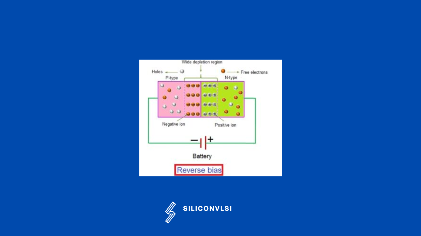
If the reverse-biased voltage applied on the p-n junction diode is further increased, then even more free electrons and holes are pulled away from the p-n junction. This increases the width of the depletion region. Hence, the width of the depletion region increases with an increase in voltage. The wide depletion region of the p-n junction diode completely blocks the majority of charge carriers. Hence, the majority of charge carriers cannot carry the electric current. The electric current carried by the minority charge carriers is very small. Hence, minority carrier current is considered negligible.
Advantages of p-n Junction Diode
- A p-n junction diode can be used to convert the alternating current (AC) to the direct current (DC).
- These diodes are used in power supply devices.
- It is much smaller.
- It needs only a smaller power to operate.
- It is cheaper.
- It can be operated with a low-voltage source.
- It is strong and not easily destroyed.
- It is used as a switch.
Why is Silicon preferred over Germanium for semiconductors?
- The main reason is, Silicon can be worked at a higher temperature as compared to germanium
- The cost of silicon semiconductors is low when compared with germanium semiconductors.
- The thermal stability of silicon is better than germanium which helps in fabrication.
- Silicon readily forms an oxide when in contact with the external environment, this helps to build the oxidation layer for the Gate terminal in the MOSFET with minimal effort and cost.
- Silicon can withstand high negative voltages
- Silicon semiconductor diodes do not allow the electric current flow if the voltage applied on the silicon diode is less than 0.7 volts.
- Germanium semiconductor diodes do not allow the electric current flow if the voltage applied on the germanium diode is less than 0.3 volts.
Application of pn junction diode || Use of pn junction diode
- LED lighting applications
- As switches in digital logic designs.
- In clipping circuits as wave shaping circuits
- In detector and demodulator circuits.
- As rectifiers in DC power supply manufacturing
- In clamping circuits in TV receivers
Types of Diodes
- Zener diode
- Avalanche diode
- Light Emitting Diode
- Laser diode
- Tunnel diode
- Schottky diode
- Varactor diode
- P-N junction diode
What is reverse biased?
Reverse bias refers to the application of an external voltage across a semiconductor diode in such a way that the positive terminal of the battery is connected to the n-side and the negative terminal is connected to the p-side of the diode.