
Interview Questions with Answers
- CMOS Inverter
- CMOS logic, give the various techniques you know to minimize Power Consumption.
- Crosstalk and Shielding
- DRAM Full Form
- Explain the sizing of the inverter in CMOS
- Gate-All-Around (GAA)
- How does the Resistance of the metal lines vary with increasing thickness and increasing length?
- Metal Semiconductor Contact
- Second-order effects in CMOS
- SRAM full form
- Tunnel Diode
- Via doubling can help to stem yield loss
- VLSI Full Form
- What are the limitations in increasing the power supply to reduce delay?
- What happens to delay if we include a resistance at the output of a CMOS circuit?
- What happens to delay if you increase load capacitance?
- What is Charge Sharing in CMOS
- What is ERC(Electrical rule checking )
- What Is Netlist?
- Which transistor has higher gain, BJT or MOS and why?
- Why do we gradually increase the size of inverters in buffer design
- Why is the substrate in NMOS connected to Ground and in PMOS to VDD?
- Why NMOS pass strong 0 and weak 1
- Why not give the output of a circuit to one large inverter?
- Why PMOS and NMOS are sized equally in Transmission Gates?
- Why PMOS pass strong 1 and weak 0
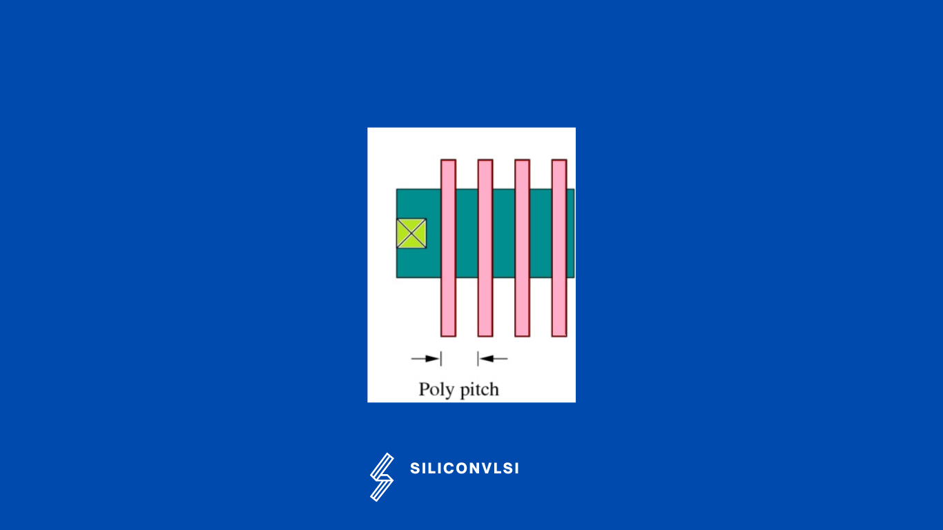
What is poly pitch?
- Poly pitch is the distance between two poly(center to center). Poly pitch is also referred to as CPP (contacted poly pitch) and interconnect pitch is also referred to as MMP (minimum metal pitch).
In which region does the MOSFET act as a current source?
- After the Vds is increased to a certain level that pinch-off occurs, the gate and the drain voltages lose control over the current flowing gate. That is, beyond that value of Vds, the current will be almost constant. we can also say that current is independent of Vds.
What are the three operating regions of MOSFET?
MOS transistors have three regions of operation:
- Cut-off Region – It is the region where the device will be in the OFF condition and there is zero amount of current flow through it.
- Saturation Region – In this region, the devices will have their drain to source current value as constant and this happens only once when the voltage across the drain to the source terminal increases more than the pinch-off voltage value. In this scenario, the device functions as a closed switch where a saturated level of current across the drain to source terminals flows.
- Linear/Ohmic Region – It is the region where the current across the drain to the source terminal enhances with the increment in the gate voltage
What happens in CMOS if we use an N substrate in the place of a P substrate?
- As we know, Nmos is faster than Pmos because electron mobility is higher than hole mobility. The effective performance of CMOS depends on the NMOS performance.
- If we create a P-well above N-type substrate, to get maximum electron mobility in NMOS, we need a very highly doping P-well, which is a costly process. So, the fastest NMOS was obtained with a high resistive P substrate.
What is a Triode region in MOSFET?
- The triode region is also called a linear region. and the amount of current which passes through a MOSFET will be a function of the voltage on the gate and drain and given gate voltage, at low drain-source voltages, the drain-source current will be proportional to the drain-source voltage (Linear mode). At higher drain-source voltages, the current will be essentially constant (Saturation mode).
What is the Hot-Electron effect in MOSFET?
- The hot electron effect is caused by high electric fields in short-channel devices. High electric fields result in high kinetic energy of electrons and some of the electrons may get enough energy and it may be trapped in between the body and the gate. This leads to deposition of negative charge on the gate which leads to an increase in threshold voltage by increasing flat band voltage. This effect is usually limited to n-channel devices because holes have much lower mobility than electrons.
What is the pinch-off condition in MOSFET?
- When the appropriate voltage is applied to the gate, a channel is formed between the source and drain and this is called a linear region, It created a pipe between the source and drain so that charges can move from the source to the drain. Next, if we apply more voltage at the drain side, then this will cause charge movement between the source and drain. But, it will also change the shape of the channel:
What is the difference between the cut-off, linear, and saturation region in the MOSFET?
- In Cutoff, Vgs < Vt (Vt: threshold value) and no current flows.
- In the Linear region, Vgs > Vt and current increase when Vgs increases.
- In saturation, the current is constant for all Vgs values. or we can say that its independent of Vds
Which is Best, P-Well or N-Well?
- N-well is superior to P-well because of lower substrate bias effects on transistor threshold voltage and lower parasitic capacitances associated with the source and drains region and also Latch-up problems can be considerably reduced by using a low resistivity epitaxial p-type substrate.
Why is nwell used in VLSI technology?
“P-Type substrate have a laser mobility(Holes), so overall substrate noise is very low if we use N-substrate than substrate noise will be more(Electrons)”
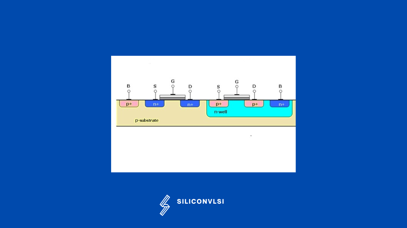
- In Complementary Metal Oxide Semiconductor(CMOS) technology, we need both P-mos and N-mos transistors to build our circuits. And more importantly, we need to fabricate both these transistors on the same silicon substrate, also called a wafer. The wafers are mostly doped p-type.
- The P-well process is preferred in circumstances where Balanced characteristics of the nMOS and pMOS are needed. It has been observed that the transistors in the native substrate tend to have better characteristics than those made in a well. Now electrons mobility is faster than hole mobility, so if we make P-well, then hole mobility again decreases. so we choose to n-well rather than P-well
- NMOS transistors are faster than PMOS transistors. So to make n channel MOS, the well must be p-type. To get the maximum electron mobility, the p should be as lightly doped as practical. If an n-type substrate were employed that would mean that the n channel MOS would be made with the addition of a p well. This p well would need to have significantly higher doping than the n-type substrate
What are the pros and cons to use p-type or n-type substrates?
- With p-type substrate allows us to build n-channel transistors without additional doping. This is a substantial advantage because, the lower the doping, the higher the mobility of electrons and the higher the gain, and the higher the switching speed of transistors we can get. Since NMOS transistors are faster than PMOS transistors, they can be used in specialty high-speed circuit blocks, so the choice of starting with a p-type substrate is probably better than starting with an n-type substrate.
What challenges did you face in lower node technologies?
- Double Patterning
- Layout-Dependent Effects
- Interconnect layers
- Design rules
- Device complexity and variation
What is an integrated circuit?
An integrated circuit is known as IC and is a complex layering of semiconductors, coppers, and other interconnected materials to form resistors, transistors, and other components
What is Dopping
The process of adding impurities to semiconductors is called doping.
What is Intrinsic and Extrinsic Semiconductor
Semiconductors that are chemically pure, in other words, free from impurities are termed intrinsic semiconductors, and the semiconductors that are doped with specific impurities is called Extrinsic Semiconductor